ESD Sensitivity Testing of Mini-Circuits ERA-4XSM
1.0 Purpose:
To determine the Electrostatic Discharge Sensitivity of Mini-Circuits Amplifier ERA4XSM in accordance with Human Body Model (HBM) and Machine Model (MM) ESD sensitivity standards. The failure criterion is: 1dB change in gain and/or 10% change in device voltage.
2.0 Ref.:
ESD STM5.1-1993 (for HBM) and ESD STM5.2-1999 (for MM).
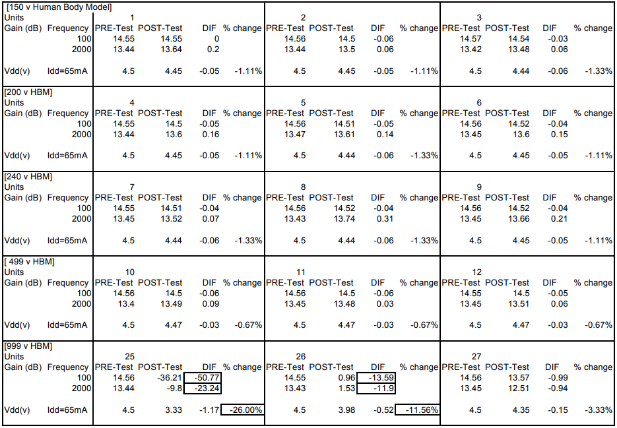
3.0 Human Body Model
Three (3) separate samples were used for each of the different values of ESD voltage: 150V, 200V, 240V, 499V, and 999V. Each sample was subjected to 3 ESD pulses of each polarity at each of 3 pairs of pins: input – output, input – ground, and output – ground, a total of 18 pulses.
Electrical performance testing was done for gain and DC device voltage at 65mA bias current, before and after the ESD pulses. Data are presented in Table 1. Using the failure criteria stated in 1.0, all devices passed at 499V; at 999V, 2 failed and 1 passed marginally.
4.0 Machine Model
4.1 Testing per ESD STM5.2-1999
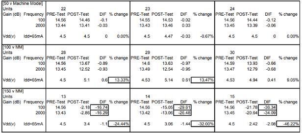
Three (3) separate samples were used for each of the different values of ESD voltage: 50V, 100V, and 150V. Each sample was subjected to 3 ESD pulses of each polarity at each of 3 pairs of pins: input – output, input – ground, and output – ground, a total of 18 pulses.
Electrical performance testing was done for gain and DC device voltage at 65mA bias current, before and after the ESD pulses. Data are presented in Table 2. Using the failure criteria stated in 1.0, the devices passed at 50V and failed at 100V.
4.2 Additional Machine Model Testing
Additional machine model testing was done in three steps, to evaluate how much performance degradation occurs when progressively increasing ESD voltage is applied to a given device, and when a given ESD voltage is applied repeatedly with performance monitored after each pulse. Separate device samples were used for each of the three steps.
1. In Step 1, one ESD pulse of each polarity was applied with fixed amplitude of 100V to the different combinations of pins in order to determine the most sensitive pair of pins and most sensitive polarity. Purpose: to reduce the amount of testing required in the subsequent tests.
2. In Step 2, a sequence of ESD pulses was applied to each device at the most sensitive pair of pins and polarity found in Step 1, one pulse at each of the following voltages increasing in value: 50V, 70V, 100V, 150V, 200V. Gain and device voltage were measured initially and after each ESD pulse.
3. In Step 3, an ESD pulse with fixed amplitude of 100V was applied multiple times, at the most sensitive pair of pins and polarity found in Step 1, in order to determine cumulative effect of ESD stress.
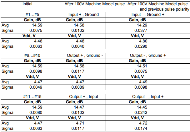
Step 1 Test.
Applying 100V ESD pulse showed the following: The most sensitive pin combination is input-to-ground where the “-” was applied to the input and “+” was applied to the ground. With that condition the gain dropped by 0.3dB and device voltage rose by 0.32V. The least sensitive pin combination is output-to-ground where the “+” was applied to the output and “-” was applied to the ground. With that condition the gain dropped by 0.08dB and device voltage rose by 0.02V. Table 3 lists the data.
Step 2 Test.
The results of progressively increasing the ESD stress, one pulse at each voltage, are shown in Figures 1 and 2.
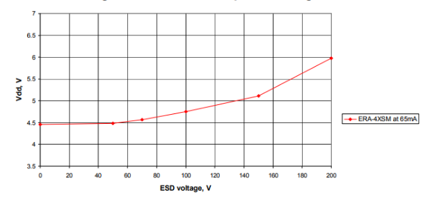
Figures 1 and 2 show that very little but still noticeable degradation in gain (0.1dB) and device voltage (0.1V) starts with the 70V ESD pulse.
At ESD pulse of 100V the changes in gain and device voltage are gradually increasing. The degradation caused by the 100V ESD pulse is in very good correlation with the Step 1 measurements that were performed on other samples of ERA-4XSM.
At ESD pulse of 150V more degradation is observed, but it is still gradual. This may be a cumulative effect rather than simply the effect of increased ESD voltage, as demonstrated by Step 3 (which was done with repeated 100V pulses).
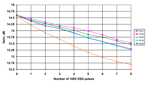
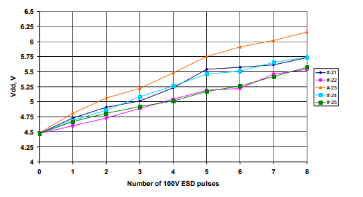
Step 3 Test.
Five units were stressed repeatedly with 100V ESD pulses. Electrical tests for gain and device voltage were made after each ESD pulse. The results are shown in Figures 3 and 4. After one pulse all 5 units passed the criteria of less than 1dB gain and less than 10% device voltage change. After 2 pulses, one failed the voltage criterion.
5.0 Conclusions
5.1 Human Body Model:
The new amplifier ERA-4XSM can withstand ESD at least up to 499V (Class 1A).
5.2 Machine Model:
The new amplifier ERA-4XSM shows gradual degradation in the gain and the device voltage. That fact is not so bad. Even with the multiple stress a customer would rather have gradual changes then catastrophic failure. The amplifier withstands a single 100V ESD pulse, or 3 pulses at 50V.