Glossary of VCO Terms
VOLTAGE CONTROLLED OSCILLATOR (VCO):
This is an oscillator designed so the output frequency can be changed by applying a voltage to its control port, also known as its tuning port.
FREQUENCY TUNING CHARACTERISTIC:
Frequency versus tuning voltage performance for a given VCO. This is usually graphed as frequency vs. voltage.
FREQUENCY VS. TEMPERATURE:
Variation of frequency with temperature at a fixed tuning voltage.
MONOTONIC TUNING:
This refers to the fact that for a given frequency voltage characteristic, the frequency is single-valued at a given voltage, and vice versa. The slope has the same sign across the tuning range.
TUNING SENSITIVITY:
This is the slope of the tuning characteristic and is expressed as frequency change per unit voltage change (MHz/V, etc.).
TUNING LINEARITY:
Tuning linearity is the deviation of the frequency versus tuning voltage characteristic from a best-fit straight line. It is sometimes called tuning nonlinearity.
TUNING OR MODULATION, AND DELTA MODULATION SENSITIVITY:
The slope of the tuning voltage characteristic at a given tuning voltage is the tuning or modulation sensitivity. The difference in modulation sensitivity at two operating tuning voltages is the delta modulation sensitivity.
TUNING SPEED (OR RESPONSE TIME):
This is the time required for the output frequency to settle to within 90 percent of its final value after applying a step change in tuning voltage. The settling time or tuning speed is related to the tuning or modulation bandwidth.
VCO INPUT CAPACITANCE:
The total equivalent capacitance seen at the tuning port of the VCO. This capacitance is a function of the DC component of the test signal applied to the tuning port, and depends mainly on the varactor diode capacitance vs. voltage characteristic.
MODULATION OR TUNING BANDWIDTH:
The modulating frequency at which the frequency deviation decreases to 0.707 of its dc value. This is an inverse function of the tuning-port capacitance, and it usually depends also on the modulating source impedance, which is typically 50 ohms.
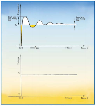
POST TUNING DRIFT:
The application of a step voltage causes the VCO to change its frequency from an initial f1 value to a final f2 value. The frequency f2 will settle to a stabilized value after some time. Post tuning drift is the frequency error compared to a final stabilized value at a specified time after the application of a step voltage. Expressed as frequency error in Hz, kHz, etc. as illustrated in Figure 1.
FREQUENCY DRIFT WITH TEMPERATURE:
This is the frequency drift of the VCO with temperature at a fixed tuning voltage, and may be expressed as a relative percentage change per unit temperature, or as a frequency change per unit temperature.
OUTPUT POWER:
The fundamental sinusoidal frequency output of the oscillator measured into a 50-ohm load, expressed in dBm.
OUTPUT POWER VARIATION:
The maximum to minimum power variation (expressed in dB) observed over the specified frequency range in a 50-ohm system at a given temperature.
OUTPUT POWER FLATNESS:
Variation of the output power from the average output power, expressed in dB.
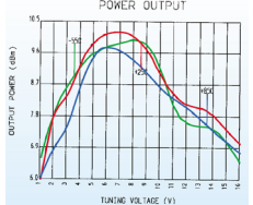
OUTPUT POWER CHANGE WITH TEMPERATURE:
The change in the output power over the temperature range. (Example using Mini-Circuits Models POS-765 or JTOS-765 is shown in Figure 2.)
FREQUENCY PUSHING:
The changing of output frequency corresponding to a given change in the supply voltage at a fixed tuning voltage (expressed in MHz per volt).
FREQUENCY PULLING:
Frequency variation caused by changes in the impedance of the output load. It is usually specified at a load return loss of 12dB and all possible phases, and is expressed in MHz peak-to-peak.
HARMONIC CONTENT OR SUPPRESSION:
Harmonic levels are measured relative to the fundamental signal (the"carrier") and expressed in dB referenced to the carrier (dBc).
SPURIOUS RESPONSES OR NON-HARMONIC SPURIOUS CONTENT:
Spurious spectral components are unwanted and non-harmonically related signals present at the oscillator output. Spurious response is usually expressed in terms of dBc.
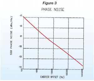
SSB PHASE NOISE:
Single side band phase noise in 1Hz bandwidth is measured relative to the carrier power at a given offset from the carrier frequency and is expressed as dBc/Hz, as illustrated in Figure 3 (Mini-Circuits models POS-1025 or JTOS-1025). For more information see Application Note relating to VCO Phase Noise.
FLICKER NOISE:
One of the sources of noise associated with solid state devices, the amplitude of which varies inversely with offset frequency. It is also referred to as 1/f noise.
RESIDUAL FM:
Alternatively known as RMS frequency error, this is another form of specifying the frequency stability of a signal source. It is the total rms frequency deviation Δfrms within a given modulation bandwidth fa to fb. The bandwidth is usually specified as 50Hz to 3kHz. Expressed mathematically, we have:
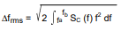
where f is the offset frequency from the carrier, and SC(f) is the single-sideband phase-noise power spectral density function.
Q OR QUALITY FACTOR:
A figure of merit often used in describing the sharpness of a tuned circuit response. A high-Q circuit has a sharper response, and vice versa. Applied to a VCO it refers to the frequency-determining resonator, and high Q improves noise suppression.
VARACTOR DIODE:
A diode operated in a reverse biased condition providing a junction capacitance that is a function of the applied reverse bias voltage.
PHASE LOCKED LOOP (PLL):
A feedback circuit in which the VCO frequency and phase are locked to the frequency and phase of a stable reference signal.
FREQUENCY SYNTHESIZER:
A system that generates any one of equally spaced frequencies within a given band, referenced to a stable frequency.
PHASE DETECTOR:
A circuit which compares two coherent RF signals and generates a DC output voltage or current that is a function of the difference between the phase of two signals.
PHASE DETECTOR GAIN:
This is a constant for a given device and given input signal conditions, and is measured in volts per radian or amperes per radian.
BODE PLOT OR BODE DIAGRAM:
A method of describing the transfer characteristic of a circuit or system where the gain function as magnitude in dB and phase shift is plotted on a logarithmic frequency scale.
UNITY GAIN:
The gain at which the magnitude of the open loop gain is equal to 1 (or 0 dB).
UNITY GAIN FREQUENCY:
The frequency at which the magnitude of the open loop gain crosses the 0dB point.
LOOP FILTER:
The loop filter is generally a low pass filter which filters the output of the phase detector and determines the noise characteristics of the VCO. If the phase detector generates a current output, then the loop filter will integrate the output signal from the phase detector into a DC voltage to drive the VCO to a specific frequency. The loop filter may take different forms, a typical one being a lag/lead network.