Measuring the electrical performance characteristics of RF/IF and microwave signal processing components
The treatment given here is introductory, and will assist the reader who wishes to consult the standard texts for further detail on measurement techniques. For measurements on mixers and frequency doublers, please refer to the applications notes on these subjects.
Linear Measurements, Passive and Active Devices
The instrumentation shown in Figure 1 can be used for a broad range of measurements on devices having one port, two ports, or many ports. Three representative devices are indicated. Properly calibrated per the instrument manufacturer's instructions, the setup will measure the following characteristics as functions of frequency:
Insertion Loss, VSWR, Gain, Isolation, Directivity, Amplitude Unbalance, Phase Unbalance, Group Delay
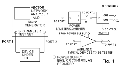
The S-parameter test set measures four sets of magnitude-and-phase quantities. When the network analyzer commands a signal to be outputted by Port 1, the signal reflected back to Port 1 by the D.U.T. (device under test) is detected and displayed as S11, while the signal passing through the D.U.T. and detected at Port 2 is displayed as S21. Similarly, a signal outputted by Port 2 yields S22, and that portion of the signal originating at Port 2 which passes through the D.U.T. to Port 1 becomes S12.
Before connecting the D.U.T., the test set is calibrated by storing reference reflection and transmission data in the network analyzer. For reflection, each cable which will later go to the D.U.T. has precision short, open, and matched load terminations successively connected to it. For transmission, the two cables are joined directly together for a "through" connection.
Now, consider a two-port D.U.T. Suppose the "input" port of the D.U.T. is connected to Port I of the test set, and the "output" is connected to Port 2. The magnitudes of S11 and S22, expressed in dB, will be negative or zero because the reflected power is less than, or at most equal to, the incident power. Dropping the minus sign the S11 and S22 dB values equal the return losses at the D.U.T. input and output ports. From there, VSWR can be calculated. A one port D.U.T. such as a termination is tested for VSWR the same way, but with only S11 being measured.
Insertion loss is measured directly as S21, and so is isolation of passive components such as switches, power splitter/combiners, and directional couplers. For amplifiers, gain is measured as S21 and reverse isolation as S12 Gain testing may require a fixed attenuator at the amplifier output to avoid overloading the detector in the S-parameter test set; suitable MCL models for this purpose are the SAT, NAT, and BW series.
Directivity of a coupler can be measured as a direct quantity by first normalizing the network analyzer for a 0 dB insertion loss reference using the main-line-input to coupled-port path through the D.U.T. The cable connected to the main-line input is then moved to the main-line output for the actual measurement. Each unused port should be connected to a matched termination, such as the MCL BTRM, STRM and NTRM series. Amplitude and phase unbalance of power splitter/combiners and multi-throw switches is measured by first normalizing insertion loss through one path, and making the actual measurement through another path. It is important to note here that whenever a D.U.T. with three or more ports is being tested, each port not actually connected to the test set must have a matched termination. This entire method requires the characteristic impedance of the S-parameter test set to be the same as that specified for the D.U.T.
Compression Measurements
Measurement of insertion-loss compression or gain compression is sufficiently similar to the corresponding linear measurements that the same setup still applies. Usually the quantity of interest is the input power (for passive devices) or output power (for amplifiers) at which the insertion loss or gain is 1 dB less than the low-power value.
When input power at 1 dB compression is the specified characteristic, the input power is set at the specified 1 dB compression value, and a 10 dB fixed attenuator is placed at the output of the D.U.T. The network analyzer is normalized for transmission response in this configuration. The 10 dB attenuator is then moved to the input of the D.U.T., and insertion loss is measured. The results show directly the amount of compression; if less than 1 dB, the device meets its specification.
The method used for testing 1 dB output power compression of amplifiers is described in applications note entitled "Automated Compression Measurements."
Intermodulation Measurements, Two-Tone Third-Order
The test setup is shown in Figure 2. Generator frequencies ("tones") are commonly set 1 MHZ apart, near the low end of the specified frequency band. The test is repeated in mid-band and near the high end. Output power of each RF generator and the net path gain or loss up to the D.U.T. are chosen to yield a specified D.U.T. output power for each tone. When the intercept point is to be calculated from the measured data, the tone levels are set so as not to saturate the D.U.T., 15 dB below the I dB compression point as a guide. It is advisable to repeat the test with 5 dB less input for each tone and recalculate the IM intercept point; agreement within 1 dB lends confidence that the setup is yielding valid data. To meet this criterion care must be taken to ensure that the test equipment itself does not
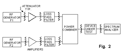
contribute too much of its own IM . The power combiners and the amplifiers and attenuators ahead of it all promote isolation between the RF generators, which could otherwise produce IM internally. The low pass filters reduce harmonics which could add to any distortion generated by the D.U.T. The attenuators before and after the filters ensure matched terminations so that the filters have their prescribed responses. The attenuator ahead of the spectrum analyzer must ensure that the analyzer is not overloaded.
To perform the measurement, set the spectrum analyzer to obtain a display like that in Figure 3. The applied tones and the IM products shown are 1 MHZ apart. The tones should be at equal amplitude, and the two third order products should be nearly equal to one another. IM suppression is read as the dB difference between the applied tones and the third-order products.
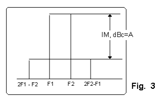
Third order intercept point is computed from this measurement as IP3 = P + A/2. If P is input power to the D.U.T., this yields input IP3 and if P is output power, output IP3 is computed.
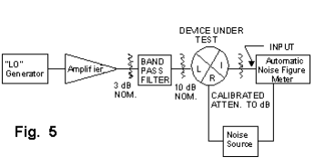
Noise Figure Measurements
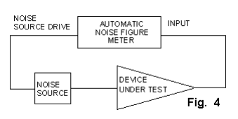
The test setup for amplifiers using an automatic noise figure meter is simple, as shown in Figure 4, although much sophistication is implemented in such an instrument. Noise figure and gain readings can be obtained by following instructions furnished by the instrument manufacturer.
For mixers an LO signal is introduced as shown in Figure 5. The band pass filter, tuned to the LO frequency, suppresses any noise sidebands falling at an IF-separation from the LO frequency. The IF commonly used is 30 MHZ. During the meter calibration sequence the noise source must be connected
directly to the input port of the noise figure meter. The 10 dB attenuator improves impedance match and measurement consistency; its value has to be subtracted from the noise figure reading. When SSB (single sideband) noise figure is the required result, 7 dB is subtracted instead.
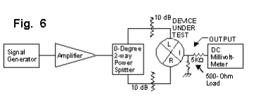
Phase Detector Measurements
Phase detectors behave similarly to mixers, but are specified for common-frequency input to the LO and RF ports. They therefore yield DC output at the port which would be the IF in a mixer. Measurements particular to phase detectors therefore pertain to the DC output: the "maximum voltage" when LO and RF signals are inphase, and the DC offset occurring when only the LO signal is applied.
Figure 6 illustrates the test set-up. A 0-degree power splitter such as Mini-Circuits' model ZFSC-2-1 applies in phase signals at +7 dBm each to the LO and RF inputs of the D.U.T. The Maximum DC Output is measured across a 500-ohm load on the output port. To measure DC Offset, disconnect the power splitter from the RF port, place matched terminations on both the D.U.T. RF port and the unused splitter output, and read the DC voltage.
Limiter Measurements
The principal limiter tests--output power and phase change with variation of input power--are readily done with the network analyzer setup in Figure 1, with these additions ahead of the D.U.T.: an amplifier having 1 dB output compression point of 30 dBm or more, followed by a variable attenuator with 14 dB or greater range in 1 dB steps. To ensure good impedance match a fixed attenuator of at least 3 dB is advisable before and after the variable attenuator.
The limiter output power depends upon the value of control current applied externally. The current is held constant during a test run, usually at the "typical" specified value, and can be of either positive or negative polarity. To run the test, the power input to the D.U.T. is first set at the minimum value to be used and a reference of 0 dB amplitude and 0 degree phase is obtained. Then, the D.U.T. input power is increased by means of the variable attenuator and the changes in amplitude and phase are read.
I & Q Modulators and Demodulators
Please refer to the "I/Q Measurements" applications note for a description of measurement methods.
QPSK Modulator Measurement
Insertion loss, VSWR, amplitude and phase unbalance are the most important characteristics. The test set-up at the beginning of this article is used, with the addition of 50-ohm current sources supplying ±20 mA bias to the two control ports.
Insertion loss is measured at all four control-current states: +20 & +20, +20 & -20, -20 & +20, and -20 & -20 mA. The worst of the readings represents the insertion loss of the device. The dB difference of the maximum and minimum insertion loss among the four states represents the amplitude unbalance. Phase unbalance is measured by normalizing the insertion phase to 0 degrees with +20 & +20 mA control current. Then, the actual phase is measured at each of the other control-current states, and the deviation from the desired phase value (90º, 180º, 270º) represents the phase unbalance. VSWR is measured the same way as for any two-port device, but at all four control-current states. The worst case represents the VSWR performance of the QPSK modulator.
Switching Speed Measurements
Switching speed is an important characteristic of components which change their transmission state in response to control signals. For PIN diode and GaAs switches, the change of state is from fully OFF to fully ON, and viceversa. The quantities related to switching speed which are most often specified are:
(l) Rise time and fall time, defined as the intervals between l0% and 90% and between 90% and 10% of the RF output amplitude respectively.
(2) Turn-on and turn-off time, defined from 50% of the control waveform transitions to 90% and 10% of the RF respectively
For digital step attenuators, switching speed is defined similarly, but 10% and 90% are taken as fractions of the RF amplitude step resulting from a change in the control signal state.
Testing technique is determined mainly on the basis of the range of switching speeds expected, and the frequency range of the RF signal. For devices using PIN diodes as the switching elements, the time intervals to be measured are typically one microsecond or more. Referring to the setup in Figure 7, the pulse generator has to furnish repetitive transitions between control levels, whether TTL or other voltage/current values as the D.U.T. requires. Control transition times should be at least an order of magnitude shorter than the D.U.T. RF transitions. Where a D.U.T. has two or more control inputs all must be supplied by the pulse generator with the correct polarities. The RF Generator is set to as high a level as will not cause compression in the D.U.T. so that the detector operates in its linear range and there is enough detected signal amplitude displayed on the oscilloscope. If the D.U.T. has more than one switched port (as in an SPDT or SP4T switch) each port not presently being tested should be terminated with a matched load. An oscilloscope bandwidth of at least 10 MHz should ensure good waveform fidelity, and its input should furnish a 50 ohm load to the detector so that the latter's own turn-off response time does not limit the measurement. If a very wideband oscilloscope is used or if the RF is at a low frequency, a lowpass filter may be needed after the detector to attenuate any RF leaking through the detector. Also, if video leakage (control break-through) at the D.U.T. output causes distortion in the observed waveform, the effect can be reduced by inserting a highpass filter ahead of the detector. This filter should pass the RF and attenuate signals below about 5 MHZ; a model from Mini-Circuits SHP or NHP series can be selected for this application.
Some differences in the test setup are necessary for measuring the speed of GaAs switches, which
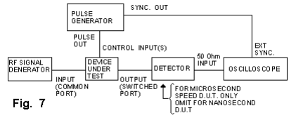
operate in the nanosecond range. Still referring to Figure 7, an oscilloscope with greater than 500 MHZ bandwidth should be used. The detector is eliminated and the switched port of the D.U.T. is connected directly to the 50 ohm oscilloscope input. The oscilloscope must be externally triggered by the pulse generator. What results is a modulated RF waveform, with a stable envelope "filled in" by the RF carrier which is not synchronized. To measure turn-on or turn-off time, a dual-trace display also showing the control signal is required, and this may involve using a wideband high-impedance probe. In any case, great care must be exercised to compensate for instrumentation path-length differences including cables (about l.5 nanoseconds per foot) and inter-channel time skew in the oscilloscope itself. Digital storage oscilloscopes have a calibration adjustment to make this compensation.