HELA-10: HIGH IP3, WIDE BAND, LINEAR POWER AMPLIFIER
1.0 Introduction
Communication systems are becoming increasingly complex. The number of simultaneous carriers used in systems such as CATV is constantly increasing. This complexity increases the inter-modulation products. In order to keep the intermodulation products under control, the carrier levels need to be lower or the system power output capability relative to the carrier level needs to be increased.
Increased output power results in a corresponding increase in DC power consumption and cost. Feed-forward amplifiers are used extensively to increase inter-modulation intercept point and thereby decrease the inter-modulation products. Feed-forward amplifiers are generally expensive and are not readily available. This application note presents a new device, HELA-10 which incorporates a pair of amplifiers providing high intercept point comparable to a feed forward amplifier, but at a significantly lower cost.
HELA-10 is very versatile, and can work in both 50- and 75-ohm systems. Four models, designated HELA-10A, HELA-10B, HELA-10C, and HELA-10D, are the same device with a choice of specifications. Each model corresponds to the device being embedded in a different set of baluns and biasing components that optimize it for 50- or 75-ohm system interfaces and different frequency ranges. This Application Note refers to the individual model numbers when distinguishing their individual performance, or simply as HELA-10 when describing their common characteristics.
2.0 HELA-10, A Balanced Power Amplifier
HELA-10 is a balanced, sixteen-lead, power amplifier with a nominal gain of 11 dB. Figure 1 is a photograph of the amplifier.
Figure 2 shows how the amplifier is used with external baluns and bias components. The amplifier is powered by a single +12V DC power supply. It operates in Class-A and produces a nominal output power of 1 watt.
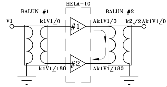
HELA –10 consists of a pair of amplifiers. As they are on the same chip, their gain and phase are very well matched. If a balanced signal is applied to the input of the HELA-10 then the output is also balanced. By using a set of baluns (or transformers) at the input and output, shown functionally in Figure 3, a single-ended input is first converted into a balanced signal in balun #1, amplified in amplifiers #1 & #2, and combined in the balun #2 to produce a single-ended output. The amplifier pair can ideally produce twice the output power of a single amplifier. Since Figure 3 presents signal levels in terms of voltage and “A” is the voltage gain of each amplifier, the √2 factor is used to indicate power doubling. Factors k1 and k2 are a function of the turns ratios and losses of baluns #1 and #2.
Amplifiers are nonlinear devices. Minimizing non-linearity of an amplifier, for a given drive level, requires good design. HELA-10 is fabricated utilizing a GaAs MESFET process. MESFETs enhances third-order distortion performance since they are generally square law devices with low third-order terms. The balanced configuration increases IP3 by 3dB over that of a single-ended amplifier, while doubling the output power at 1-dB compression.
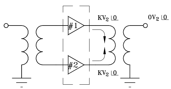
Figure 4 shows how the balanced configuration provides second-order cancellation, yielding outstanding IP2 performance. This is due to phase cancellation in the balanced circuit, whereby the second harmonic does not appear at the output of the second balun. The same is true for all even harmonics. In reality, the amplifiers and baluns are not perfect; thus a small amount of even harmonic is present. HELA-10 has an excellent second-order intercept of 88 dBm typical when used with specified Mini-Circuits baluns.
3.0 Specifications and Performance
Table 1 lists the electrical specifications of the amplifier at room temperature. Power output is typically 30 dBm in all four configurations. A unique feature of the HELA-10 amplifier is its ability to work in both 50- and 75-ohm systems depending upon the baluns chosen, as shown in the table in Figure 2.
All the referenced graphs and conclusions cover the entire circuit which includes the baluns and the biasing circuits described in 2.0. This amplifier, as well as the transformers used as baluns, are housed in surface mount packages making this set of components ideally suited to pick-and-place and high volume production.
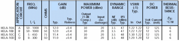
This table is for guidance only. See Mini-Circuits catalog for full specifications. Performance includes the effect of the respective application circuits; see Figure 2 for details. Thermal resistance is from junction to heat slug, or mounting paddle.
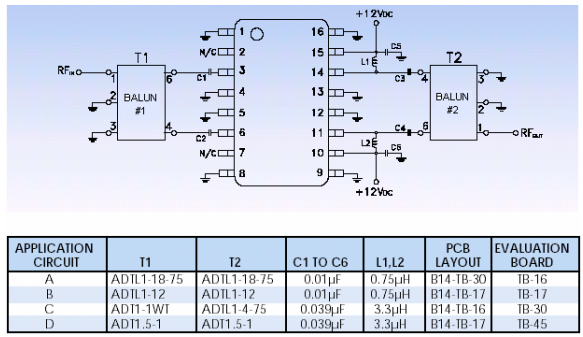
Balun Pin 2 connection is not required for:
T1 and T2 of HELA-10A and HELA-10B, T2 of HELA-10C.
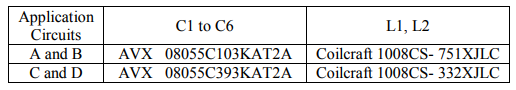
Kits are available containing HELA-10 and transformers for the Application Circuits.
Suggested manufacturers’ part numbers for the remaining components:
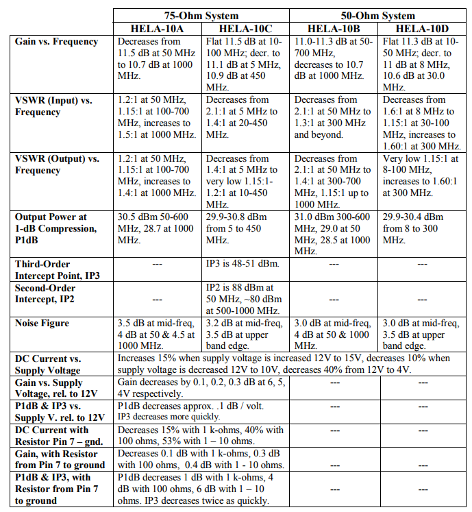
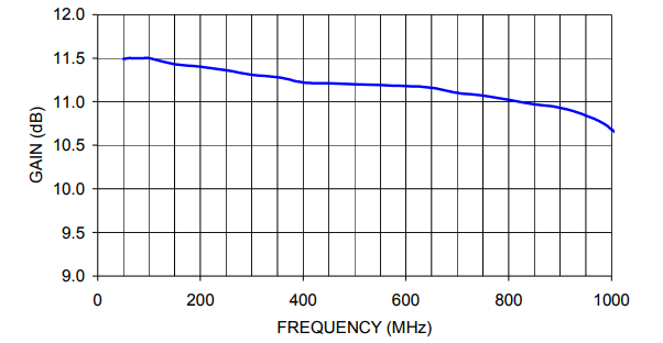
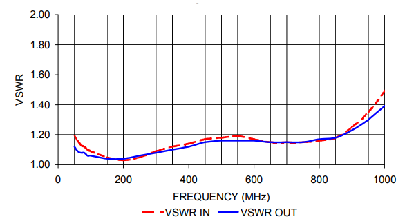
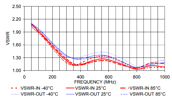
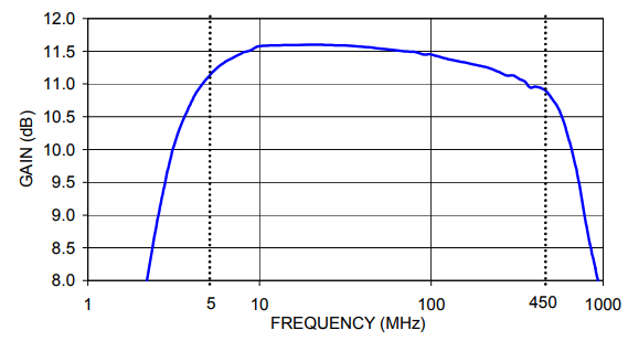
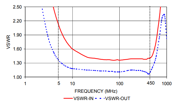
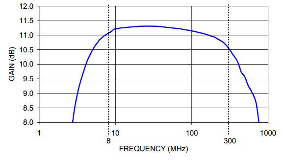
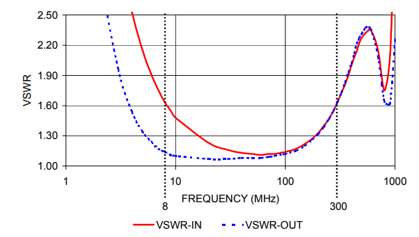
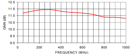
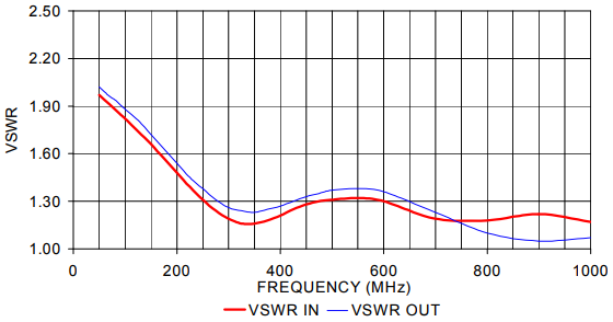
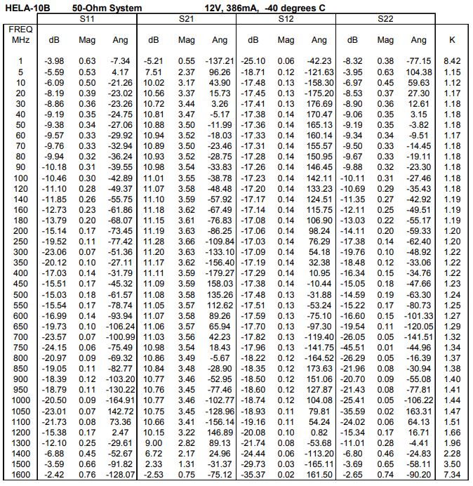
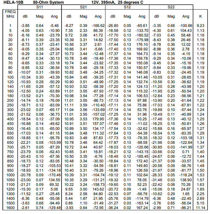
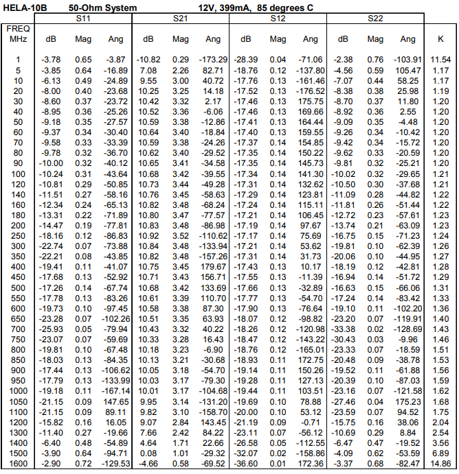
Figures 5 through 12 show the gain and VSWR of HELA-10 in each of the configurations HELA-10A through HELA-10D. Gain is extremely flat, typically within ±0.3 to ±0.4 dB. This is an excellent feature for wideband systems. The VSWR is typically 1.15:1 to 1.3:1 over most of the respective frequency bands, and is determined largely by the baluns. The excellent match of the 75-ohm HELA-10A, for example, meets the stringent matching requirements of a CATV amplifier. For the 50-ohm HELA-10B, port matching is excellent above 300 MHz. Below 300 MHz, the VSWR increases to a manageable 2:1 at 50 MHz. The curves for HELA-10B in Figures 7 and 8 include performance at 3 ambient temperatures: -40, 25, and 85°C. Gain change with temperature is about ±0.3 dB at low frequency, increasing to about ±0.6 dB at 1000 MHz. VSWR changes with temperature are very small.
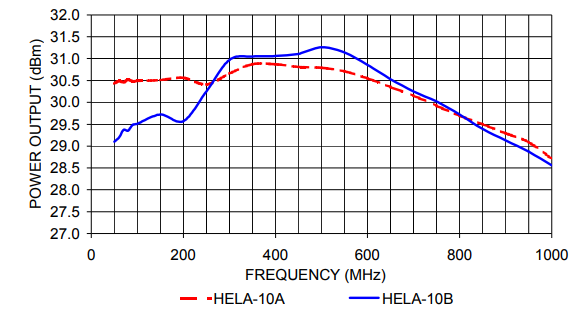
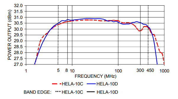
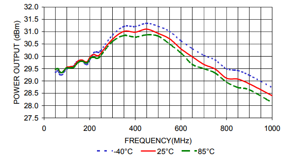
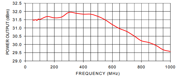
Figure 13 shows typical output power at 1-dB compression for HELA-10A and HELA-10B; Figure 14 shows it for HELA-10C and HELA-10D. For HELA-10A output power is about 30.5 dBm up to 600 MHz and tapers to 28.7 dBm at 1000 MHz. For HELA-10B output power peaks above 31 dBm at 500 MHz and decreases to 29.0 and 28.5 dBm at the 50 and 1000 MHz band edges. For HELA10C it stays around 30 dBm across the 5 to 450 MHz range. For HELA-10D output power is 30 dBm up to about 400 MHz. Figure 15 shows how HELA-10B output power varies with temperature: hardly at all at low frequency, and typically ±0.35 dB at 1000 MHz.
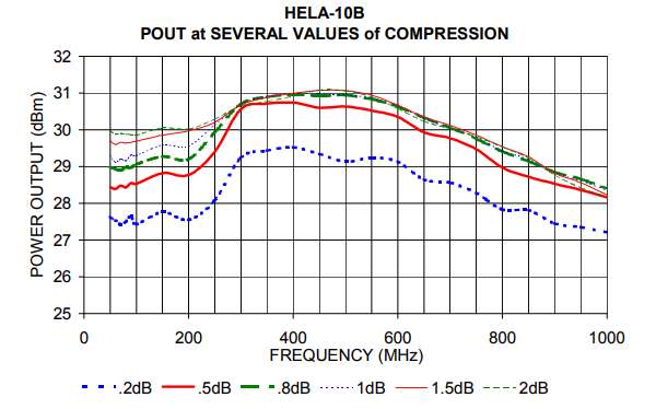
So far, output power at 1-dB compression has been described. Figure 16 shows output power of HELA-10B at several steps of gain compression: 0.2 dB through 2.0 dB. From 300 to 1000 MHz the curves for 0.5 dB and greater compression values group together, indicating that the amplifier does not have to be driven hard to obtain high output power. This is significant for satisfying the needs of highlinearity, low distortion applications.
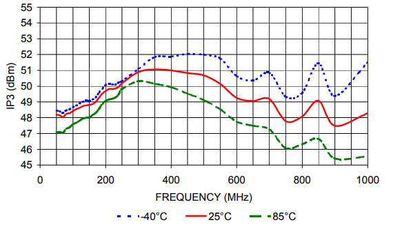
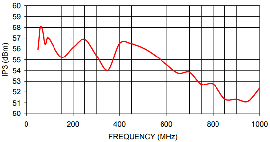
Figure 17 shows the output third-order intercept point (IP3) of HELA-10B at three temperatures. At room ambient IP3 is typically 48 to 51 dB. IP3 of amplifiers is, in general, 10 dB above 1 dB compression. Comparing Figures 15 and 17, it is seen that for HELA-10, IP3 is typically 19 – 20 dB above 1 dB compression across the frequency range. This is equivalent to using 10-watt amplifier. High IP3 is of great advantage when using this amplifier in multi-carrier systems.
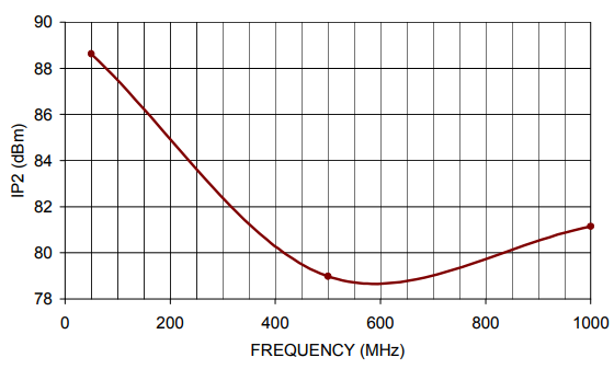
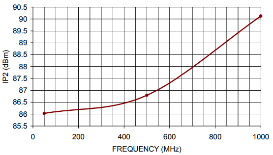
Another important distortion measure is the output second-order intercept (IP2), shown in Figure 18 for HELA-10B. IP2 is typically 88 dBm at 50 MHz, and around 80 dBm over the upper half of the band.
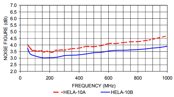
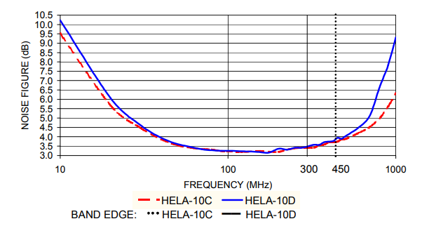
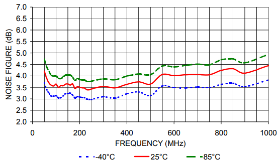
Noise figure of HELA-10A and HELA-10B is shown in Figure 19, and HELA-10C and HEAL-10D in Figure 20. Noise Figure over temperature for HELA-10B is in Figure 19. Typically, noise figure is 3.0 to 3.5 dB in the mid-frequency range. For HELA-10A and HELA-10B it increases to 4.0 – 4.5 dB at 1000 MHz; for HELA10C and HELA-10D it remains quite constant from about 80 MHz to the top of their respective frequency bands. Figure 21 shows noise figure over temperature; it varies typically 0.008 dB/°C.
3.1 Typical Performance at Different Values of Supply Voltage
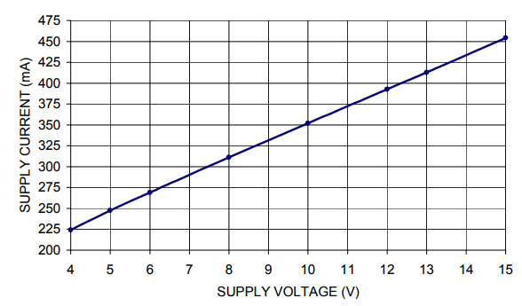
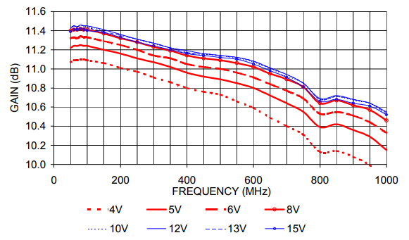
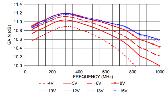
HELA-10 can also be used at different supply voltages, at the user’s discretion; the performance is not guaranteed by Mini-Circuits. Figure 22 shows that DC current varies proportionally with voltage. Figures 23 (HELA-10A) and 24 (HELA-10B) show that the gain is nearly constant with voltage, especially in the range 8 to 15V.
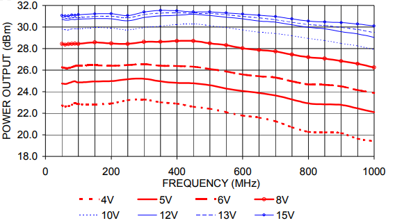
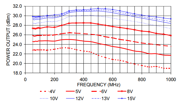
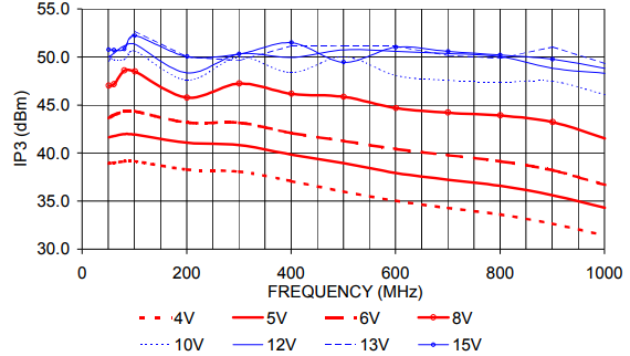
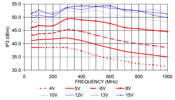
Output power at 1-dB compression, shown in Figure 25 for HELA-10A and in Figure 26 for HELA-10B is affected by supply voltage, giving the user a trade-off of DC power and signal power handling capacity. Third-order intercept point (IP3) is shown in Figures 27 and 28 for HELA-10A and HELA-10B respectively. At supply voltages 10 to 15V, IP3 is about 19 dB above the 1-dB compression power for HELA-10A, and for HELA-10B it is about 23 dB above throughout the frequency range. At lower supply voltages the difference between IP3 and output at 1-dB compression is less, especially at the higher frequencies; at 4V it is about 15 dB up to 500 MHz, and 10 – 13 dB at 1000 MHz.
3.2 Performance summary
Table 2 summarizes the typical electrical performance in 50-ohm and 75-ohm systems (25°C). It includes results from Sections 3.0 and 3.1, as well as Section 4.1.
A Word of Caution:
Data points and curves for 15V supply voltage are included for reference only, as reliable performance above the 13V maximum voltage rating cannot be guaranteed. The 15V curves mainly show that little or no performance advantage accrues from operating above 13V.
4.0 HELA-10 as a Cascaded Amplifier
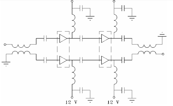
For higher gain applications, a driver amplifier is required. It has not been easy to find a driver having sufficiently high IP3 since the driver contributes to the overall IP3. HELA-10 is a cascadable amplifier, thus it can also be used as a driver. Figure 29 shows the schematic block diagram of a two stage, cascaded HELA-10 amplifier. A typical gain of 20 dB can be achieved using this cascade.
A direct cascade could have a disadvantage in power consumption, which would be twice that of a single amplifier. But, HELA-10 has an intelligent biasing scheme to overcome this. By connecting an external shunt resistance from Pin 7 to ground the supply current can be controlled in the driver stage of a cascade. This biasing feature can also serve to reduce the current consumption when HELA-10 is used for other low power applications.
4.1 Typical Performance, Supply Current Control via Shunt Resistance
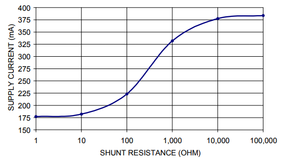
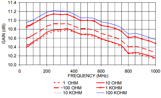
The graphs described in this section show performance using a 12V DC supply, with current reduced by connecting an external shunt resistor from Pin 7 to ground. The purpose is to show a trade-off available: reduced DC current consumption against output power and intermodulation performance. Figure 30 plots the supply current of a typical amplifier as a function of shunt resistance, demonstrating for example, that the current can be reduced by about half by using a resistor of 10 ohms or less.
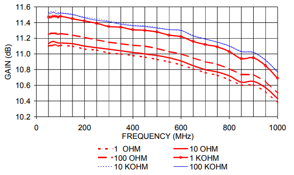
Gain varies by only about 0.5 dB over the entire range of resistance, as shown in Figure 31 for HELA-10A and Figure 32 for HELA-10B.
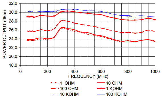
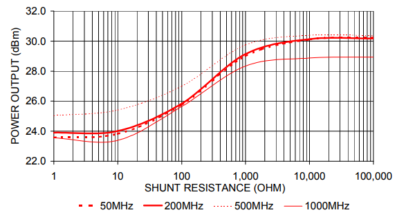
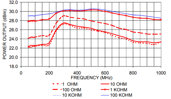
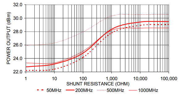
Power output at 1-dB compression is presented two ways: swept-frequency with resistance as parameter, and versus resistance with frequency as parameter. The graphs for HELA-10A are in Figures 33 and 34, and the graphs for HELA-10B are in Figures 35 and 36. They show that the user can exercise a 4 – 6 dB trade-off of output power against supply current. For example, a bias resistor of 100 ohms typically reduces current consumption by 100 mA. It still produces a HELA-10A power output of 26 dBm, more than adequate as a driver.
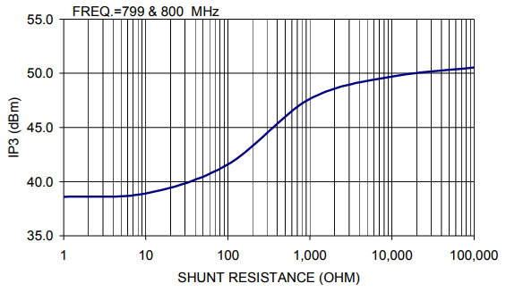
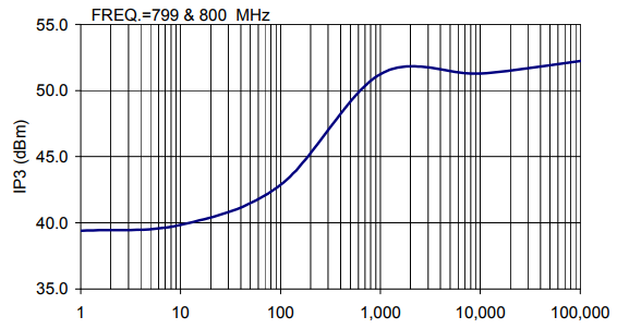
Third-order intercept point (IP3) is shown in Figures 37 and 38 as a function of shunt resistance, for 2-tone signal at 799 and 800 MHz. At resistance values corresponding to high supply current, IP3 is typically 50 – 51 dBm, which is about 21 – 22 dB above the 1-dB compression level. At resistances corresponding to low supply current, IP3 is typically 39 dBm, which is about 15 dB above 1-dB compression.
4.2 Typical Performance at Higher Supply Current
As an extension of the work reported in 4.1 where current was reduced, this section describes performance obtained when current is increased to typically 525 mA. Instead of a shunt resistor from Pin 7 to ground, the increase is obtained using a voltage divider: 2430 ohms from the 12V supply to Pin 7, and 365 ohms from Pin 7 to ground. The trade-off in this case provides increased output power and improved intermodulation performance with higher current consumption.
Typical performance with this arrangement is shown for HELA-10B (50-ohm system) in Figures 39 through 43. We will compare it with the 25°C curve in the graphs for HELA-10B operating with no connection to Pin 7 (390 mA typical).
Gain, comparing Figures 39 and 7, is about 0.2 dB greater at the higher current. Input and Output VSWR, comparing Figures 40 and 8, is virtually the same. Output Power at 1-dB Compression, comparing Figures 41 and 15, is typically 1 dB greater at the higher current. A larger improvement in Third Order Intercept Point (IP3) is seen at the higher current, typically 3 dB comparing Figures 42 and 17. For Second Order Intercept Point (IP2), Figures 43 and 18 indicate that the low point in the frequency band is typically 7 dB greater at the higher current.
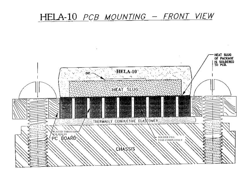
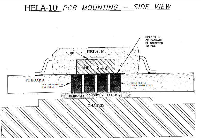
5.0 Layout and Thermal Aspects
The PCB layout for the HELA-10 amplifier must consider both the electrical requirements of the parts (proper line impedance, bypassing, etc.) and the thermal requirements. The thermal requirement, to meet the stated MTTF of better than 800 years, states that the maximum temperature of the heat slug on the bottom of the HELA-10 package is 110°C. There are three different thermal interfaces between the bottom of the HELA-10 and the chassis. The first is the solder connection of the HELA-10 heat slug to the PCB. The second interface is the heat transfer through the PCB, and the third is the PCB to chassis interface. These interfaces are shown in Figures 45 and 46, which illustrate how the HELA-10 is mounted.
The first interface, the solder connection of the HELA-10 heat slug to the PCB, should cover the full area of the HELA-10 heat slug for maximum effectiveness.
The mounting system, including the PCB, must be designed for the maximum expected system ambient temperature. To do this, the following two parameters need to be known: the maximum external ambient temperature and the temperature rise of the chassis above the external ambient temperature.
Once these two parameters are known the maximum temperature rise between the chassis and the HELA-10 can easily be calculated.
Maximum Temperature Rise (°C), Chassis to HELA-10 slug =
110 – maximum external temperature – chassis rise
For example if: Maximum external temperature = 60°C, and Chassis rise due to internal heating = 20°C
Then: Maximum Temperature Rise (°C), Chassis to HELA-10 slug = 110 – 60 – 20 = 30°C.
In the above example a 30°C rise is allowed in the PCB mount between the bottom of the HELA-10 slug and the chassis. Knowing this, the second and third interfaces need to be designed to provide a thermal resistance which will maintain a 30°C or less temperature rise.
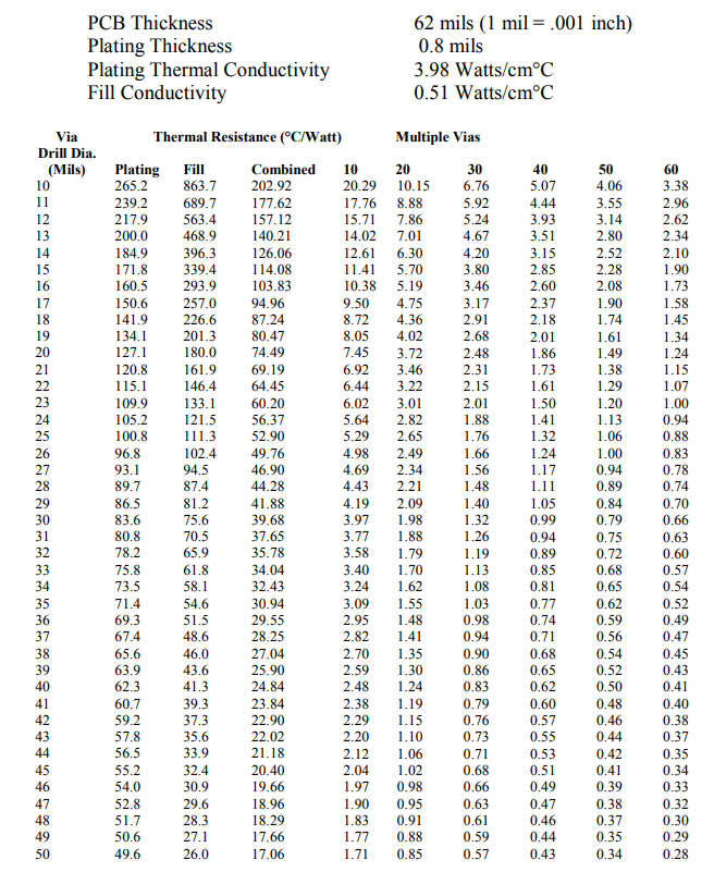
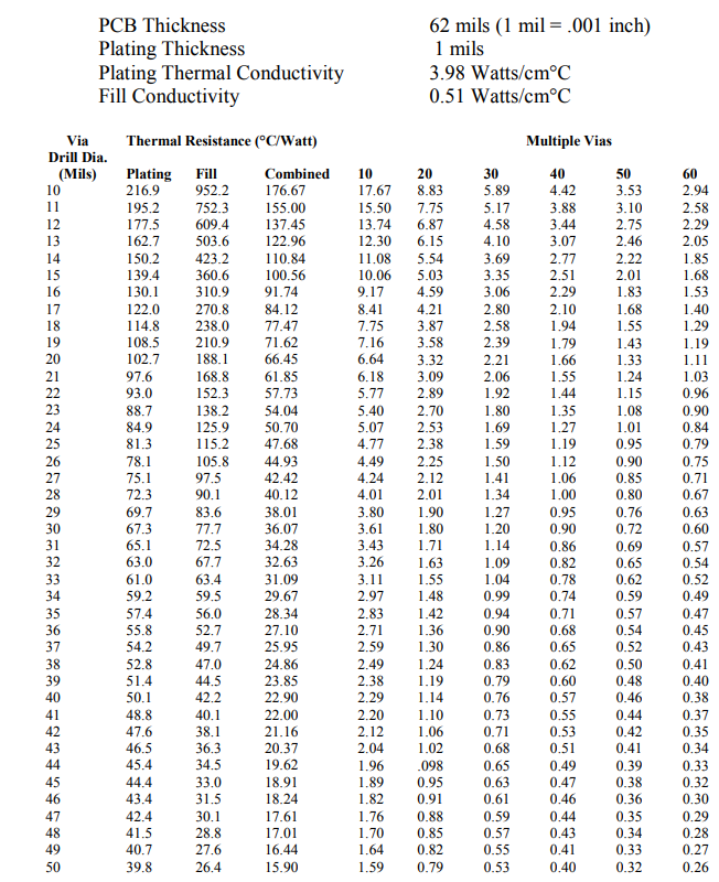
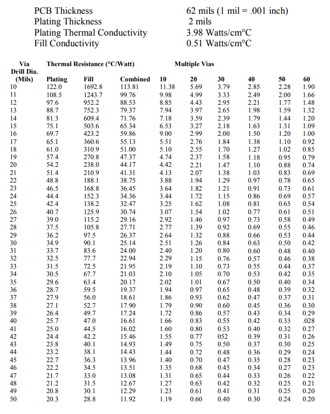
The second interface is the heat transfer through the PCB. FR4, the typical PCB material used in most applications, has very poor thermal conduction properties and cannot be used without the addition of via (through) holes under the HELA-10. The via holes should be copper plated and then solder filled for the lowest thermal resistance. The via holes then conduct the heat through the FR4 to the bottom of the PCB, while the FR4 material provides the mechanical support. The thermal resistance of the via holes, given in degree C rise per watt of power dissipation, is a function of via diameter and the thickness of the copper plating on the walls of the via holes. Tables 3, 4, 5 show the calculated thermal resistance of a solder-filled, plated through via hole with different via diameters and copper plating thicknesses. Table 3 shows the thermal resistance with 0.8 mil copper plating, Table 4 with 1 mil, and Table 5 with 2 mil copper plating. The thermal resistance of the copper plating alone is shown in the column Plating, the thermal resistance of the solder fill is shown in the next column, and the column labeled “combined” shows the calculated thermal resistance of the copper plating and the solder fill together, for a single via. The next columns show the thermal resistance achieved by using multiple via holes.
As an example, a 32 mil diameter via with 2 mil thick copper plating has the following properties:
Thermal resistance of the copper plating = 32.5°C / watt
Thermal resistance of the solder fill = 77.7°C / watt
Combined thermal resistance of single via, which is the parallel combination of the above = 22.94°C / watt
A thermal resistance of 22.94°C / Watt would produce a 145°C rise with 6.3 Watts of power dissipation (HELA-10) and therefore a single via cannot be used. As more via holes are added, the combined thermal resistance decreases quickly and is determined the same way as for parallel resistors. If we use 36 such via holes the total thermal resistance will be only 0.64°C per Watt and the temperature rise though the PCB will be only 4°C. The actual via diameter, thickness of the copper plating, and number of via holes used will be determined by the limits of the PCB manufacturing process used.
The third interface is between the PCB and the chassis. Note that the chassis is considered to be an infinite heat sink in this application note. Unlike the HELA-10 to PCB interface, this cannot be a solder connection due to the mismatch in thermal expansion of the PCB and chassis material and other production limitations. A thermally conductive elastomer or gasket material is recommended. One such material that may be applicable for this application is Thermagon, Inc.’s T-PLI 200 material. This material is a thermally conductive, conformable elastomer that is available in either sheet form or cut to size.
The thermally conductive elastomer should conform to any irregularities on the PCB and chassis surfaces caused by the manufacturing process, while providing a low thermal resistance. A sheet thickness of 20 mils appears to be the best compromise between thermal resistance, tolerance build-up, and handling. The 20 mil thick material has a stated thermal resistance of 0.14°C – in2 per Watt. Using a square area of 0.1 square inches at this interface and a power dissipation of 6.3 watts, a temperature rise of 8.8°C is expected. The PCB should be attached to the chassis with screws, providing a slight compression of the elastomer material. Users must determine if this material is acceptable for their application.
5.1 Operating Ambient Temperature Range using a Test Board
As a practical example, temperature rise of the HELA-10 above room-ambient temperature was measured with the unit mounted in Mini-Circuits Test Board TB17 (which characterizes it as HELA-10B). It would be desirable to measure the temperature of the heat slug, but it is difficult to do this directly because of the way the unit must be mounted for heat sinking. Therefore, measurement proceeded as follows.
Ambient temperature = 27°C
Case temperature (measured at the top of the plastic body) = 56°C
DC Supply Voltage = 12V
DC current = 0.39A
Temperature rise, case above ambient = 56 – 27 = 29°C
Power dissipated = 12 × 0.39 = 4.68W
Thermal resistance, case-to ambient = 29 / 4.68 = 6.2°C/W
To maintain the heat slug at a maximum temperature of 110°C for best reliability, the maximum ambient temperature Tmax for the Test Board is calculated as:
T = (Maximum heat slug temperature) – (Supply voltage) × (Maximum specified DC current) × (Thermal resistance, case-to-ambient) – 5°C
In this formula 5°C is a margin accounting for having measured case temperature instead of heat slug temperature. Substituting the values in this example:
Tmax = 110°C – 12V × 0.525A × 6.2 – 5 = 66°C.
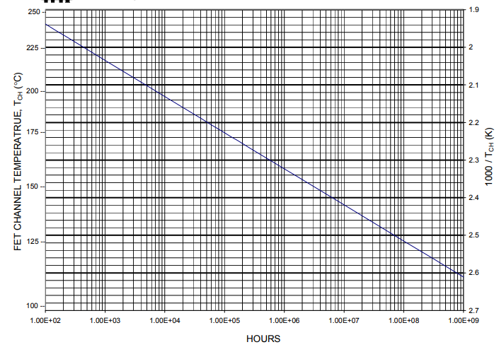
For reference, the FET channel temperature in HELA-10 can be estimated under those conditions:
Tch = (Maximum heat slug temperature) + (Supply voltage) × (Maximum specified DC current) × (Thermal resistance, channel-to-heat slug) = 110°C + 12V × 0.525A × 6.0 = 148°C.
From Figure 44, the corresponding MTTF is 3 × 10⁶ hours.
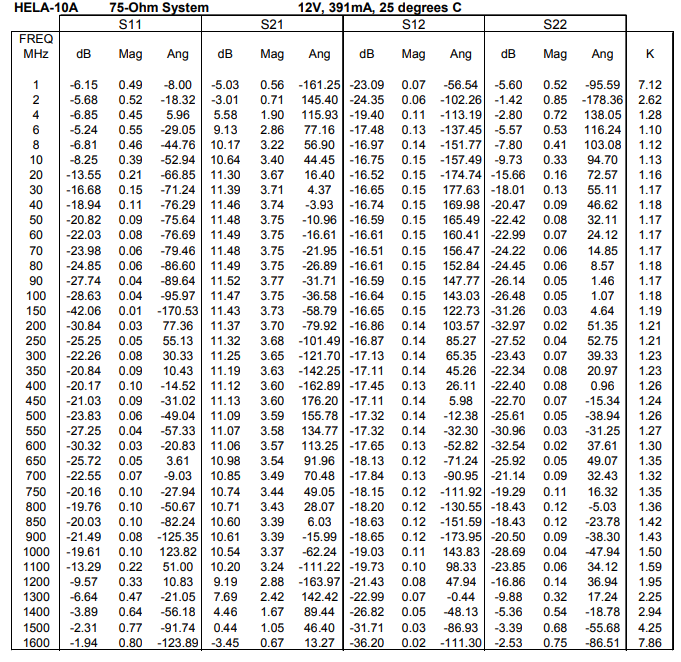
6.0 Typical S-parameters
Tables 6 through 9 list typical s-parameters of HELA-10A (75-ohm system) and HELA-10B (50-ohm system). For HELA-10B there are three separate tables: for –40, 25, and 85°C. These s-parameters include the effect of the baluns and biasing components shown in Figure 2. From the tables it is evident that HELA-10 is unconditionally stable.
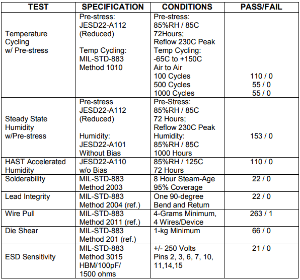
7.0 Environmental Capabilities and Mean-Time-to-Failure (MTTF)
As part of qualification, the HELA-10 amplifier in its 16-lead SOIC package has passed environmental tests as listed in Table 10.
Figure 44 shows how MTTF varies with FET channel temperature in HELA-10. The slope in the graph corresponds to an activation energy of 2.0 eV.
The MTTF is a guideline only and merely reflects Mini-Circuits opinion or commendation of the model as it is not appropriate to predict linearly the life expectancy of a model strictly based on MTTF and junction temperature. Other factors such as ambient temperature, heat dissipation, current and voltage applied and length of use of the model are just a few factors that also need to be considered.
Accordingly, the MTTF does not constitute or create a warranty, express or implied, including, without limitation, any warranty of future performance or the life expectancy of the model.
8.0 Transients on the Bias Line
Large voltage transients on the DC bias lines can damage the HELA-10 amplifier. Suddenly connecting or disconnecting, or even momentarily shorting the DC bias to the device can generate such transients. The rapid change in the supply current results in very large voltage transients on the DC bias line due to the circuit inductance, as V = L × di/dt.
To reduce voltage transients, take the precaution of adding a Transient Voltage Suppressor (TVS) on the DC bias line. This part should be installed between the location of the power supply discontinuity and the HELA-10, the closer to the amplifier the better. A part should be selected with a nominal breakdown voltage of 15VDC. The Series SMBJ TVS from Microsemi may work for this application. For example, Part No. SMBJ13A is listed as having a breakdown voltage of 14.4V minimum and 15.9V maximum at 1mA, and a maximum clamping voltage of 21.5V at 27.9A peak pulse current. It is a 600W surface mount device in a DO214AA case. The use of a TVS is required if DC bias discontinuities are expected. The use of TVS and the bias line decoupling capacitors will prevent voltage transients from damaging the amplifier.
9.0 Conclusion
HELA-10 is a versatile one watt high IP3 (45 dBm) and IP2 (88 dBm) low cost monolithic amplifier. External baluns are required. Balun sets as well as amplifier test boards are offered by Mini-Circuits. The amplifiers are cascadable and perform equally well in 75-ohm and 50-ohm systems. HELA-10 can also be used as a high IP3 low power driver amplifier with reduced maximum power out capability. As a driver, it has a low current mode built into its biasing circuit in order to reduce DC power consumption.