BIASING OF CONSTANT CURRENT MMIC AMPLIFIERS (e.g., ERA SERIES)
Introduction
The Mini-Circuits family of microwave monolithic integrated circuit (MMIC) Darlington amplifiers offers the RF designer multi-stage performance in packages that look like a discrete transistor. Included in this family are the model prefixes to which the biasing considerations in this application note apply: ERA, Gali, LEE, MAR, MAV, RAM, and VAM. These amplifiers’ advantages of wide bandwidth, impedance match, and a choice of gain and output power levels result from their being monolithic circuits, most of which contain InGaP HBT (indium-gallium-phosphide heterojunction bipolar transistors). In addition, most of these amplifiers incorporate a patented circuit (US Patent No. 6943629) that provides protection against damage due to power supply turn-on transients.
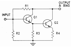
The internal circuit configuration is a Darlington pair, embedded in a resistor network as shown in the schematic diagram, Figure 1. Applying DC power to operate this kind of amplifier is simpler than biasing a transistor. Like a discrete bipolar transistor, this circuit is current-controlled rather than voltage-controlled. This means that for a range of current around a recommended value, the device voltage varies much less than in proportion to current. A constant-current DC source would be ideal for providing a stable operating point. By contrast, with most of these models the use of a constantvoltage DC source would cause the current to vary widely with small changes in supply voltage, temperature change, and device-to-device variations. Stable operating point needs an external series resistor between the amplifier and a DC voltage supply to approximate a constant-current source. This application note gives the user step-bystep guidance in choosing external bias circuit components to obtain optimum performance.
A Darlington amplifier is a 2-port device: RF input, and combined RF output and bias input. It is housed in a 4-lead package including 2 ground leads; connecting both of them to external ground will minimize common path impedance for best RF performance. Internal resistors in Figure 1 determine the DC operating point of the transistors and provide feedback to set RF gain, bandwidth, and input and output impedances to optimum values.
Bias Circuit
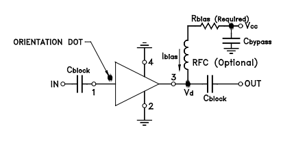
A practical biasing configuration is shown in Figure 2. Bias current is delivered from a voltage supply Vcc through the resistor Rbias and the RF choke (inductor), shown as RFC in the figure. The resistor reduces the effect of device voltage (Vd) variation on the bias current by approximating a current source.
Blocking capacitors are needed at the input anPd output ports. They should be of a type having low ESR (effective series resistance), and should have reactance low enough not to affect insertion loss or VSWR adversely at low frequency. The blocking capacitors must be free of parasitic resonance up to the highest operating frequency. Use of a bypass capacitor at the VCC end of Rbias is advised to prevent stray coupling from or to other signal processing components via the DC supply line.
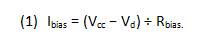
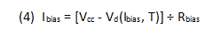
Bias current is given by the equation:
The individual data sheet for each of the amplifiers lists the values of the bias resistor needed with several values of supply voltage. These values take into account the variation of device voltage, both lot-to-lot and with temperature (-45° to 85°C). Also, they are chosen from the readily available “1%” resistor values. The greater the difference between the supply and device voltage, the easier it is to maintain constant operating conditions; this will be discussed. A further consideration affecting component choice is the DC power dissipated by the bias resistor, which increases with increasing supply voltage.
The bias current values in the data sheets are the recommended values. Greater current raises junction temperature, reducing MTTF (mean time to failure). The effect of bias current on MTTF is discussed in more detail later.
Advantage of an RF Choke
The advisability of using an RF choke in series with Rbias is evident from the following analysis. Figure 3 shows an equivalent circuit of the output of a Darlington amplifier as a current source in parallel with an internal 50-ohm source resistance, loaded by both Rbias and an external 50-ohm load. The current in the 50-ohm load is:
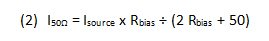
and the loss in power gain relative to not having the output loaded by Rbias is:

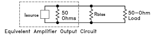
Suppose, for example, that Model ERA-4SM+ is used with a 12-volt supply without a choke. From the above expression, the effect of the 115-ohm bias resistor (from the data sheet) is found to be a 1.7 dB reduction in the gain of the amplifier.
An RF choke should be chosen such that its reactance is at least 500 ohms (10 times the load impedance) at the lowest operating frequency. It must also be free of parasitic (series) resonance up to the highest operating frequency.
Super Wide-band RF Choke
The circuit designer might consider using a commercially available inductor as the RF choke in the bias circuit of Figure 2. The low end of the useful frequency range is controlled by the value of the inductance; the higher the value, the lower the frequency. The high end of the frequency range is determined by the series resonant frequency of the inductor; it tends to decrease as the value of the inductance increases. The frequency band of the overall amplifier circuit is often limited by the inductor rather than the MMIC amplifier itself, which have performance up to 8 GHz. Besides, inductors are not clearly specified for RF choke application, and design change by the inductor manufacturer will have an unknown effect on the circuit. This complicates the circuit designer’s job.
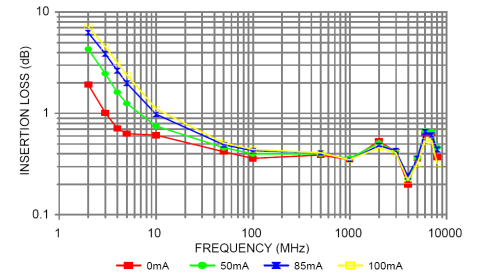
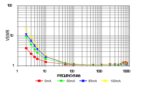
Mini-Circuits solves the problem by offering super wide-band RF chokes, which enable circuit designers to utilize easily the full capability of the MMIC Darlington amplifiers. An RF choke is a 2-terminal device. In a 0.31 by 0.22-inch surface mount package, models ADCH-80+ and ADCH-80A+ cover 50 to 10000 MHz with different pin-outs to accommodate different PC board layouts. In a smaller 0.15 by 0.15-inch package, TCCH-80+ covers 50 to 8200 MHz.
The equivalent inductance of the Super Wide-band RF choke ADCH-80+ is one microhenry at 100 mA. For comparison, a typical commercially available one microhenry inductor has a series resonant frequency as low as 90 MHz, which is much lower than this RF choke. Figure 4 plots the insertion loss and Figure 5 the VSWR at various currents up to 100 mA, for the RF choke placed in shunt across a 50-ohm transmission line. Note that the insertion loss and VSWR change very little with change in current in the specified frequency band.
Higher Bias Resistor Values Reduce Variation
Increasing the supply voltage allows a higher value of Rbias to be used, in accordance with the pertinent data sheet, and that reduces the variation in bias current. The benefit is that RF performance, especially the 1-dB compression point, is made more constant. The following quantifies this effect.
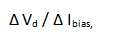
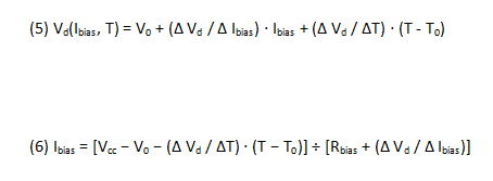
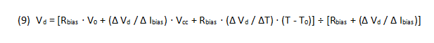
The device voltage Vd is a function of both Ibias and temperature T. Device voltage increases with bias current, and the variation can be expressed as a rate of change:
in mV per mA. Device voltage in most models decreases with increasing temperature, as:

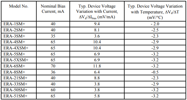
in millivolts per degree C. Over the useful range of bias current and temperature, these rates of change can be assumed constant. Typical values of these variation coefficients for the ERA series are listed in Table 1 as examples. This information is for applications guidance only; for the latest specifications refer to published data sheets where you can find the values of the coefficients for all Mini-Circuits MMIC Darlington amplifiers.
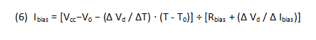
The combined effect of the two device-voltage coefficients can be expressed as variation of bias current with temperature, derived as follows:
where:

The “∆” ratios are the respective device-voltage vs. current and device-voltage vs. temperature coefficients. V0 is the Vd-axis intercept of the linear extension of the Vd vs. Ibias curve, at room temperature T0. Substituting for Vd from (5) into (4) and solving for Ibias:
Differentiating (6) with respect to T gives the desired result:
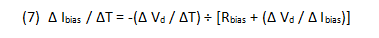
To find the change in bias current that will typically occur with a given change in temperature ∆T, substitute values for the device-voltage coefficients from Table 1 or the data sheet for the model, and the value of bias resistor being considered, into the right-hand side of equation (7). Multiplying the result by ∆T yields the change in bias current ∆ Ibias over the temperature range.
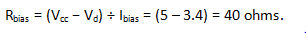
To illustrate how the choice of supply voltage affects the variation of bias current with temperature, let us compare two values of Vcc for Model ERA-1SM+.
For the first example, Vcc = 5 volts, find Rbias by inverting equation (1):
Substituting in equation (7):

Over an operating temperature range of −45 to 85 degrees C, the total variation in current for this example will be 5.2 mA, which is 13% of the recommended value of current. The consequence is about 1.4 dB variation in output power at 1-dB compression.
For the second example, let Vcc = 12 volts and Rbias = 215 ohms. A similar calculation yields 1.16 mA total variation in current, which causes only 0.4 dB variation in output power.
Additional Sources of Variation
The variation of device voltage as discussed above pertains to an individual device. The specifications include the limits of device voltage that the various models must meet. Actual expected unit-to-unit variation is much less than indicated by those limits, because of the high degree of process control used during manufacture. Therefore, a user can be confident that results obtained when prototyping products incorporating Mini-Circuits MMIC Darlington amplifiers that performance will be highly repeatable. Besides the variation of bias current due to the characteristics of the amplifier itself, there are two additional causes that the user might need to consider:
- Available nominal values, tolerance and temperature coefficient of the bias resistor.
- Voltage setting error and regulation of the power supply.
Resistors readily available are generally the “1% values”. The nominal values, having increments of 2%, could thus differ from the data-sheet values by as much as ±1%. If a resistor having temperature coefficient of 200 ppm/°C is used, it could vary ±1.3% relative to the room-temperature value over the -45 to 85°C range. The resistance, and correspondingly the bias current, might therefore be as much as 2.3% different from the desired value in data sheet due to these contributions.
Good DC power supplies typically have about 10 mV combined line and load regulation, and that tends not to be an important factor. However, the tolerance of a fixed-voltage supply, or setting accuracy of a field adjustable one might be ±1%. As an example, consider the ERA-51SM+ being used with a 9-volt supply. Since the nominal device voltage is 4.5 V (half the supply voltage), a 1%, error in supply voltage would change the current by 0.5%.
The combination of the resistor and power supply variations in the above example would cause 2.3% + 0.5% = 2.8% error in current, which is 1.8 mA for a nominal value of 65 mA. Besides, the temperature effect on current in the ERA-51SM+ device itself, using equation (7), is:

Relative to the room temperature value, current would change 0.042 mA/°C × 65°C = 2.7 mA with temperature. The overall combined variation, including the bias resistor and power supply effects, is ±4.5 mA for this example. A user working within an MTTF or current consumption budget who needs to ensure that 65 mA is not exceeded may therefore choose to design for a nominal value of 60 mA in this example.
Minimizing Power Dissipation
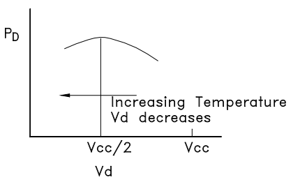
In addition to bias current stability, stability of power dissipation of the MMIC Darlington amplifier is favored by using a high Vcc value. This is because of the negative temperature coefficient of device voltage Vd. In particular, if Vcc is at least 2 times Vd, then PD, the power dissipation decreases with increasing temperature, as shown by the following analysis:
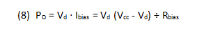
Taking the derivative of PD with respect to Vd and setting it equal to zero, we find that the maximum value of PD occurs when Vd = Vcc ÷ 2. This is illustrated in Figure 6.
Let us see what happens to power dissipation in the case of ERA-4SM+ between 25 and 85 degrees C, for two values of supply voltage: one less than, and another greater than, twice the value of Vd. We will use 65 mA and 4.6 V as the nominal (room temperature) values of Ibias and Vd.
To find the change in PD, the power dissipation of the amplifier, we must use the equations for Vd and Ibias with which we started in order to account for the interdependence of these quantities as well as temperature:
as before.
Substituting for Ibias from equation (6) into the Vd equation (5), and solving for Vd:
PD can now obtained as the product of right-hand sides of equations (6) and (9). The constant V0 is found by subtracting [Ibias x (∆ Vd /∆ Ibias)] from Vd, using the room-temperature values of Ibias and Vd.
For Vcc = 5.0 V, Rbias = 7.7 ohms. Using the value −2.9mV/°C for the Vd temperature coefficient from Table 1 and the above equations, PD increases from 0.293 watt at 25°C to 0.331 watt at 85°C. Considering the thermal resistance of ERA-4SM+ (junction-tocase) of 196°C/W, this increase in power dissipation results in 7°C higher junction temperature than if dissipation were constant. The consequence in reliability is a factor of 2 reduction in MTTF.
Now, try Vcc = 12 V, for which Rbias = 115 ohms. For this case, PD decreases from 0.293watt at 25°C to 0.288 watt at 85°C.
Temperature Compensated Bias Networ k
An alternative method of biasing that allows use of lower supply voltage while maintaining bias current stability and reducing power dissipation in the bias resistor is to use a temperature compensating bias network in place of the single resistor Rbias. The network consists of a linear positive-temperature-coefficient chip thermistor in parallel with a regular chip resistor, and should be designed so that its resistance increases with temperature just enough to make up for the decrease in device voltage, causing the bias current to remain constant.
An alternative method of biasing that allows use of lower supply voltage while maintaining bias current stability and reducing power dissipation in the bias resistor is to use a temperature compensating bias network in place of the single resistor Rbias. The network consists of a linear positive-temperature-coefficient chip thermistor in parallel with a regular chip resistor, and should be designed so that its resistance increases with temperature just enough to make up for the decrease in device voltage, causing the bias current to remain constant.
We now derive the values of the network components. Let R be the resistance of the regular resistor, and Rt the 25°C resistance of the thermistor.
Let kb be the fractional increase in Rbias needed at the maximum operating temperature relative to 25°C: (hot resistance − 25°C resistance) ÷ 25°C resistance.
Let kt be the fractional increase in resistance of the thermistor, (4500 Η10-6 ) x (maximum operating temperature – 25°C).
Because the resistor and thermistor are in parallel they must satisfy:
and
Solving (10) and (11) yields:
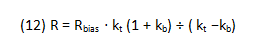
and
Let us compare simple resistor biasing with the temperature compensating network for biasing an ERA-6SM+ with a 7.0 V supply. Let Ibias = 70 mA and Vd = 4.9 V (at 25°C), and use the Rbias value 30.1 ohms from the ERA-6SM+ data sheet. If we use an ordinary resistor for Rbias without a thermistor, the current will increase to 74 mA.
Now, we compute the network component values needed to make the current 70 mA at 85°C as well as at 25°C. At 85°C, Vd = 4.9 –(0.0031 V/ °C ) x (60°C) = 4.71V, and Rbias should become 32.7 ohms. Thus, kb = (32.7 − 30.1) ÷ 30.1 = 0.0864. Also, kt = (4500 x10-6) x (85° - 25°) = 0.27. Applying equations (12) and (13),
R = 30.1 x 0.27 (1 + 0.0864) ÷(0.27− 0.0864) = 48.1 ohms
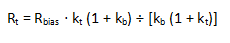
Rt = 30.1 x 0.27 (1 + 0.0864) ÷ [0.0864 (1 + 0.27)] = 80.5 ohms
If the thermistors are available only in “5% values”, sufficiently close compensation is obtained by using Rt = 82 ohms and R = 47.5 ohms (for 30.1-ohm parallel equivalent).
For different supply voltages and device operating points different resistor and thermistor values are needed, but the same concept and method can be used. The benefit is the ability to keep the device current constant over temperature, thereby avoiding increase in power dissipated in the amplifier and reduction in MTTF.
We have not mentioned the resistance-temperature coefficient of the ordinary resistor in the bias network. The reason is that thick film chip resistors typically have a coefficient of ±100 ppm/°C. This is about 2% of the TCR of the thermistor, and does not influence the results significantly. A word of caution is due regarding the thermistor, however. Its temperature characteristic is controlled only at 25°C and at 75°C. The user should test actual circuit operation at other temperatures of interest.