Low Profile, Low Cost, Fully Integrated Monolithic Microwave Amplifiers
Introduction
Monolithic microwave amplifiers are widely used in the industry for signal amplification. The majority of these amplifiers are specified to operate with fixed current. In the real world of low voltage supplies, fixed current is difficult to realize. Normally, a constant-current source is approximated by a voltage source, RF choke and a resistor. In addition, DC blocking capacitors need to be added at the input and output of such amplifiers. All these external elements consume real estate on the user’s PC board, and increase the component count, cost and complexity of the design. To address these issues, Mini-Circuits is introducing a series of fully integrated amplifiers, which operate with a fixed voltage source. Besides being easy to use, these amplifiers have very low profile and extremely high isolation. The later feature helps an amplifier to be used as an active isolator. This article presents the performance and describes the advantages of this new series of amplifiers.
Biasing of Monolithic Microwave Amplifiers
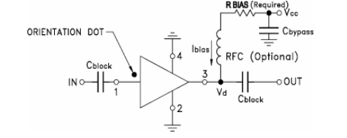
Fig 1 shows the biasing circuit of most of the commercially available monolithic amplifiers. These amplifiers are designed for fixed current operation, and the DC bias current has to be applied at the RF output terminal. Therefore, it is important to ensure that the biasing circuit does not load the RF output (by proper selection of RFC and Rbias), and that the DC current does not go to the RF load (Cblock prevents it). The combined reactance of RFC and Rbias should be greater than 500 ohms to prevent reduction of gain and power output. The RFC should also have its resonant frequency higher than the intended frequency of operation. In addition, a DC blocking capacitor is needed at the input to prevent DC current flow back into the signal source. A minimum of 2 V drop across Rbias is required for proper operation.
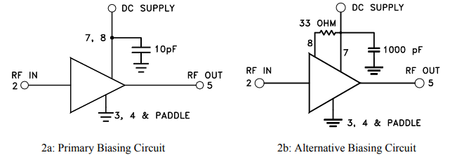
The new MNA series of monolithic microwave amplifiers that Mini-Circuits is introducing are well matched to 50 ohms; they are wide band and much simpler to use. This makes them very user friendly. Unlike current-operated amplifiers, the new series has separate terminals for the RF output and DC supply. In addition, these new amplifiers are designed to operate with a fixed voltage source rather than a fixed current source. Fig 2a shows the primary biasing circuit of the new amplifier series. Note that the only external component is a bypass capacitor for the DC supply, which provides an RF ground at the amplifier DC terminal. The capacitor, as well as the short between Pins 7 and 8 should be located as close as possible to the MNA amplifier. To ensure unconditional stability (a concern only for Model MNA-4), the alternative biasing circuit in Fig 2b is recommended. This alternative circuit has the advantage, for all models, of preventing possible resonance between internal and external biasing components. Chip components of 0402 or 0603 size are recommended, and should be located within 100 mils (2.5mm) of the amplifier package. A Test Board that includes the Fig 2b biasing circuit is available; the Mini-Circuits Specification Sheet shows the recommended PC board layout. The effect of biasing circuit on electrical performance is described later in this Application Note.
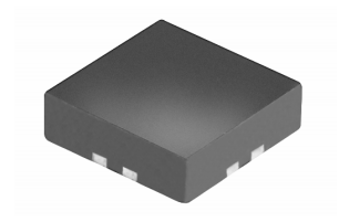
The physical dimensions of these amplifiers are 3mm x 3mm x 0.89mm, or 0.118” x 0.118” x 0.035”. This small size saves board space. The MNA amplifiers have a bottom paddle, which is soldered directly to the PC board of the customer’s circuit to provide lowest thermal resistance. Fig 3 illustrates the new MNA amplifier.
Electrical Performance
Table 1 shows the typical specifications of these amplifiers. One significant feature is that they can be operated over a wide voltage range, 2.8 to 5V. This makes them useable for battery powered applications.
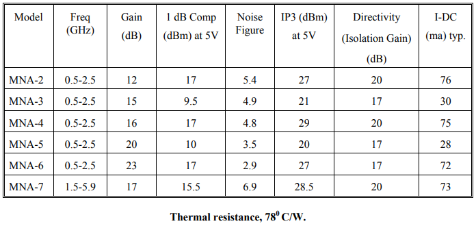
The MNA series offers a choice of gains and power output to aid the circuit designer. Detailed specifications of these amplifiers can be found at the Mini-Circuits web site:
http://www.minicircuits.com
MNA-7 is a high frequency amplifier operating over 1.5 to 5.9GHz. This wide frequency range covers applications from PCS at the low end to satellite communication at the high end, and a variety of other applications in between such as defense, ISM etc. MNA-7 has all the features of its low frequency counterparts.
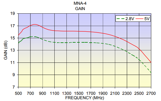
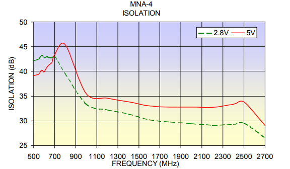
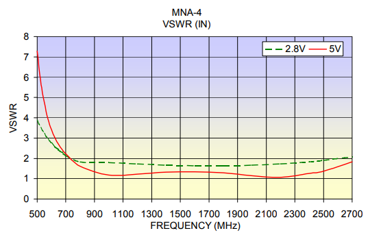
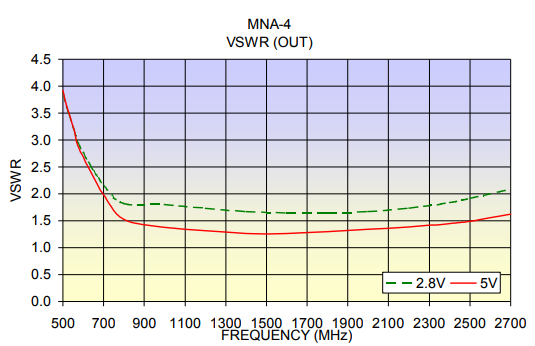
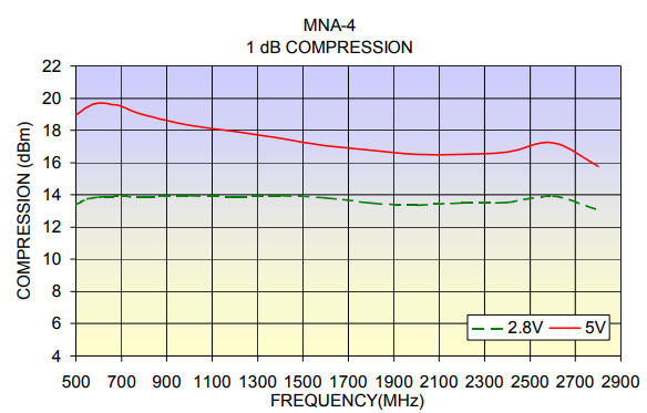
Fig 4 shows the gain of the MNA-4 amplifier, for example, at two different voltages: 2.8 and 5V. Note that the gain change is only 2dB for such a drastic change of supply voltage. Fig 5 shows the reverse isolation of the same amplifier; it is in the range of 30 to 45dB across the band. This is equivalent to an active directivity of 15 to 30dB, which enables these amplifiers to be used as low cost active isolators. Some applications for high isolation amplifiers are reducing load pull of voltage controlled oscillators, providing a broadband interface at the input and output of filters that are reflective in their stop-bands, and any situation where mismatch could degrade system performance. Figs 6 and 7 show the VSWR at input and output. The amplifiers are well matched over 700 to 2500 MHz. This makes them extremely simple to use. Fig 8 shows the 1-dB output power compression of the MNA-4 amplifier.
Note that the trade-off of output power with choice of supply voltage is well defined; the difference is about 5dB at low frequency and 2.5dB at the high frequency.
Effect of Biasing Circuit on Electrical Performance
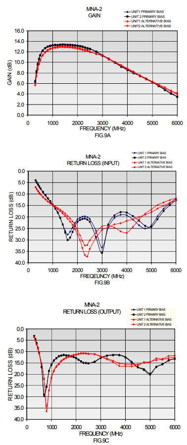
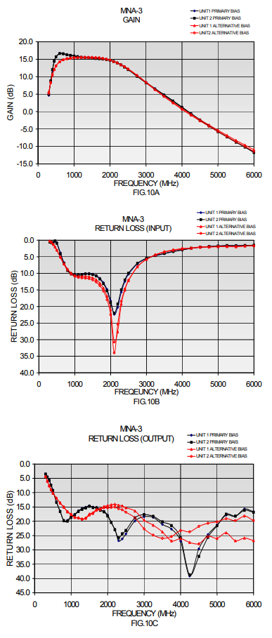
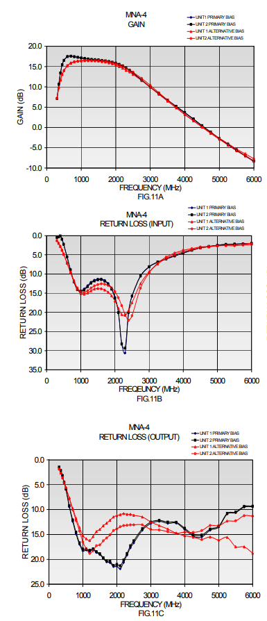
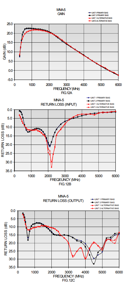
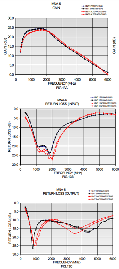
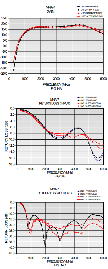
Figs 9a, b, c through 14a, b, c show gain, input return loss, and output return loss of Models MNA-2 through MNA-7 vs. frequency out to 6 GHz. Each graph plots the performance of 2 samples using the primary bias circuit (Fig 2a), as well as the same 2 samples using the alternative biasing circuit (Fig.2b).
MNA-2 and MNA-6 have slightly lower gain up to 3 GHz and up to 2 GHz respectively, with the alternative biasing circuit. MNA-3, MNA-4, and MNA-5 show decreased gain with the alternative biasing circuit only below 1 GHz, and the effect is to smooth the response by eliminating a tendency of the gain to peak. MNA-7 does not show a significant difference in the gain, but the alternative biasing circuit provides smoother return loss response at high frequencies.
Reliability
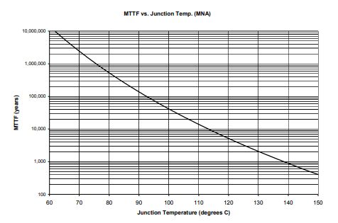
The thermal resistance of these amplifiers, from junction to case, is 780 C/W. For the 17-dBm output MNA amplifiers this results in a junction temperature rise of 35° C above the case. At 85° C case temperature the junction temperature is thus 120° C, which makes the amplifier extremely reliable. When soldered on a PCB the amplifier case temperature typically rises 100 C above ambient, making the junction temperature 130° C. From Fig 15 the MTTF is around 2000 years at this temperature. For the lower power MNA models, junction temperature is lower so there is no need for concern about MTTF, as it is extremely high.
Conclusions
Mini-Circuits has introduced a series of new amplifiers to cover 0.5 to 5.9 GHz. These amplifiers have a separate terminal for DC, and require no external matching, biasing or DC blocking elements. They operate with fixed DC voltage and have very high reverse isolation. These tiny amplifiers will save circuit space and are simpler to use.