Uses and Advantages of "MERA" Dual Matched MMIC Amplifiers
Introduction
The Mini-Circuits ERA and Gali series of amplifiers are monolithic HBT devices in Darlington configuration. They are wide band 50-ohm amplifiers that are easy to use, as they require very few external components. Wide band applications such as cable TV require excellent second-order distortion product cancellation. This can be accomplished with a push-pull amplifier utilizing a pair of amplifiers ideally identical in gain and phase. Combining two amplifiers in one package and picking adjacent dice from the wafer for this purpose satisfies the criteria of matching. These amplifiers are also useful where balanced amplifiers are needed to increase output power and IP3, or to improve impedance match (using 90-degree hybrids at input and output).
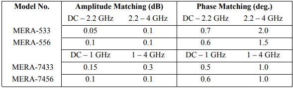
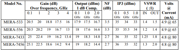
Four matched-pair medium-power amplifiers in Mini-Circuits Leadless Package (MCLP) are being introduced. Models MERA-533 and MERA-556 have typically 20 dB gain and 18 dBm output power at 1-dB compression, while MERA-7433 and MERA-7456 have typically 25 dB gain and 19 dBm output. The last two digits signify the package size: "33" for 3.25mm x 3.25mm (Case Style DL805) and "56" for 5mm x 6mm package (Case Style DL1020). Each of these packages has a ground paddle on which the two die are mounted, and which is exposed on the bottom of the package. Grounding the package by soldering the paddle to the user's PC board minimizes the thermal resistance from ambient to the case. On Mini-Circuits' evaluation board, the temperature rise above ambient is typically only 8°C or less.
This application note discusses performance including a description of the test setup for measuring the amplitude and phase balance of the amplifiers, as well as PC board layout and mounting considerations for good thermal and RF grounding design.
Performance
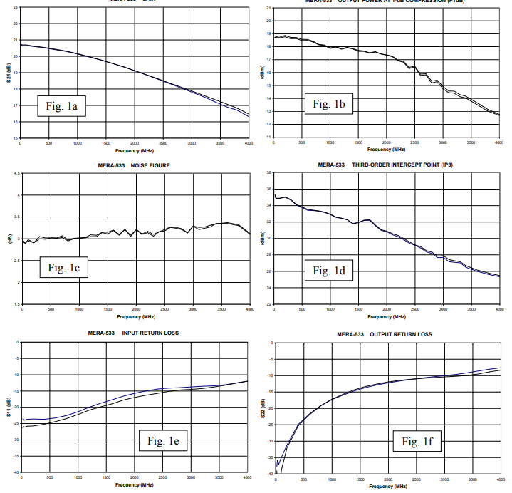
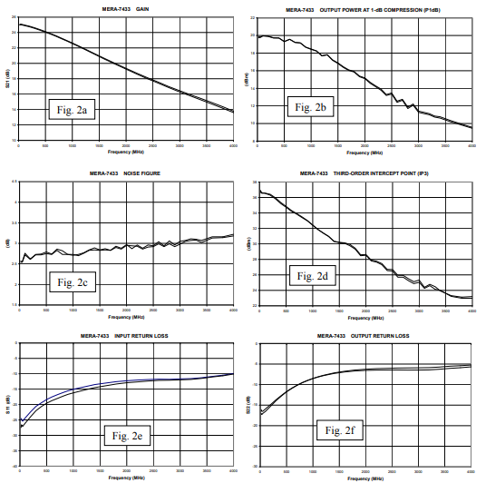
Figures 1 and 2 show the typical performance of the MERA-533 and MERA-7433 amplifiers respectively, at 25°C. All of the graphs are plotted up to 4000 MHz for easy comparison. Each graph contains 2 curves, one for each of the 2 amplifiers within the unit, and illustrates how well matched they are.
Gain (Figures 1a and 2a), P1dB (1b and 2b), Noise Figure (1c and 2c), and IP3 (1d and 2d) correspond closely to the values listed in the table above.
Specified frequency range for MERA-533 is DC - 4 GHz; at 2 GHz mid-band frequency the Input and Output Return Loss in Figures 1e and 1f are 16 dB and 12 dB respectively, corresponding to VSWR of 1.4:1 at the input and 1.67:1 at the output. The difference from the 1.5:1 VSWR-OUT value in the table is due to test fixture limitation.
Specified frequency range for MERA-7433 is DC - 1 GHz; at 0.5 GHz mid-band frequency the Input and Output Return Loss in Figures 2e and 2f are 19.5 dB and 11.5 dB respectively, corresponding to VSWR of 1.24:1 and 1.73:1; these values are close to those in the table.
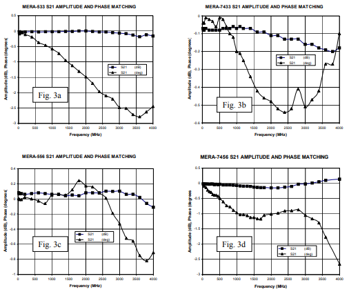
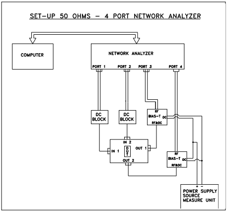
Typical matching of gain amplitude and phase is shown in Figure 3 for all four models (1 unit of each). The test setup for making these measurements is diagrammed in Figure 4. It uses a 4-channel network analyzer, Agilent ENA Series model E5071B or equivalent. An external DC Block such as Mini-Circuits BLK-18 is used at each of the two Input ports of the device under test (DUT), and a Bias Tee such as Mini-Circuits ZFBT-6GW at each of the Output ports. The Source-Measure Unit is set to provide the required bias current: 65 mA for MERA-533 and MERA-556, or 80 mA for MERA7433 and MERA-7456; it can simultaneously measure voltage of the DUT.
Thermal Considerations
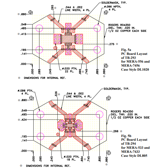
Proper heat sinking of MERA amplifiers is essential for control of temperature rise, in order to ensure that the devices are maintained within the specified case temperature range over a useful range of ambient temperature. This is particularly so because of the inclusion of 2 medium power amplifiers within a compact package, in which the DC power is dissipated in a small area. Mini-Circuits has built test boards - TB-293 for MERA-556 and MERA-7456, and TB-294 for MERA-533 and MERA-7433 - that provide the necessary heat sinking as well as RF grounding. Figure 5 shows the PC board patterns and dimensions used in the test boards. Copper covers the entire back surface of the boards. Copper thickness on each side is nominally 2 mils, due to 1/2-oz (0.7 mil) laminate plus build-up due to the process of plating at least 1 mil through the holes (PTH). As used in TB-293 and TB-294, the boards are soldered to a solid brass housing.
An important feature of the PC board design is the array of PTH via holes, which are used both for heat sinking and RF grounding. They should be filled with solder when the user mounts the board, to reduce thermal resistance. The solder connection of the MERA paddle to the PCB should cover the full area of the paddle for maximum effectiveness.
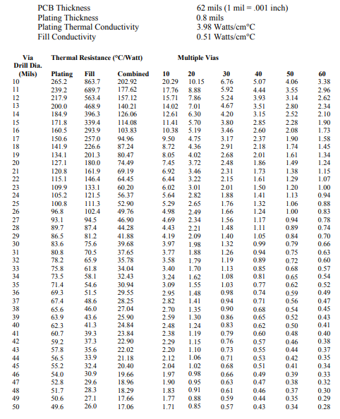
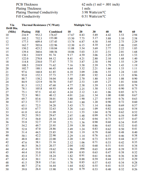
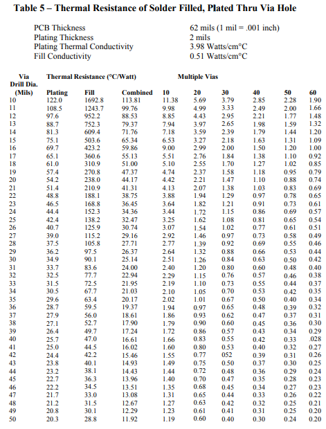
The thermal resistance of via holes, given in degrees-C rise per watt of power dissipation, is a function of via diameter and the thickness of the copper plating on the walls of the via holes. Tables 3, 4, and 5 show the calculated thermal resistance of a solder-filled, plated through via hole with different via diameters and copper plating thicknesses. Table 3 shows the thermal resistance with 0.8-mil copper plating, Table 4 with 1-mil, and Table 5 with 2-mil copper plating. The thermal resistance of the copper plating alone is shown in the column "Plating", the thermal resistance of the solder fill is shown in the next column, and the column labeled "combined" shows the calculated thermal resistance of the copper plating and the solder fill together, for a single via. The next columns show the thermal resistance achieved by using multiple via holes. The tables are based on board thickness (and thus via length) of .062 inch.
As an example from Table 4, a 20-mil diameter via with 1-mil thick copper plating has the following properties:
- Thermal resistance of the copper plating = 102.7°C / watt
- Thermal resistance of the solder fill = 188.1°C / watt
Combined thermal resistance of a single via, which is the parallel combination of the above, is 66.43°C / watt.
A thermal resistance of 66.43°C / watt would produce a 41.5°C rise with .625 watt of power dissipation (typical of MERA-556, for example) and therefore a single via will not provide optimum thermal design. As more via holes are added, the combined thermal resistance decreases quickly and the resultant is determined the same way as for parallel resistors. If we use 12 such via holes the total thermal resistance will be only 5.54°C per watt and the temperature rise though the PC board will be only 3.5°C.
Taking the example a step further, if a PC board having .020-inch thick dielectric is used as in test boards TB-293 and TB-294, instead of the .062 thickness in Tables 3, 4, and 5, the length of the vias will be .020/.062 as much, and the thermal resistance and temperature rise will be proportionally less: 1.79°C per watt and 1.1°C respectively. The actual via diameter, thickness of the copper plating, and number of via holes used will be affected by the limits of the PCB manufacturing process used.
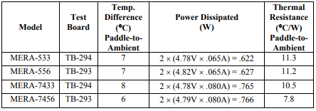
Temperature rise of the MERA amplifiers mounted on the test boards from ambient air to the paddle has been measured, and from the results the paddle-to-ambient thermal resistance values were calculated. They are given in Table 6. The variation in thermal resistance values is partly due to limitation in positioning a thermocouple to measure paddle temperature. A conservative estimate from the data would be 12°C/W for all four models.
To emphasize the importance of heat sinking in the manner described above, temperature rise was also measured for comparison using a 2-inch square PC board having a 1-inch square copper pattern on the top surface and 1-inch square ground plane on the bottom. Copper weight was 1-oz (instead of 1/2 oz) and dielectric was .059-inch FR4 (instead of .020-inch RO4350). An array of .016-diameter PTH spaced .035-inch apart (instead of .020-diameter spaced .060-inch) was used. It was found that increasing the size of the copper square beyond 1 inch did not reduce the temperature rise significantly. The main difference in this test is the omission of the solid metal backing. The results are in Table 7.
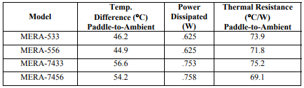
These paddle-to-ambient thermal resistance values average about 7 times as much paddle-to-ambient thermal resistance as in Table 6 for test boards TB293 and TB-294. The specified maximum operating case (paddle) temperature for these models is 85°C. Taking MERA-556 as an example, the maximum operating ambient temperature using a PC board design and solid housing like TB-293 would be 85 - 7 =78°C. The .059-inch thick FR4 board without solid metal backing would allow only 85 - 44.9 = 40°C maximum ambient.
While not tested, it is anticipated that a multi-layer PC board having a heat-conducting core would yield intermediate thermal performance.
Applications
MERA amplifiers are very useful in applications requiring the closely matched amplitude and phase characteristics given in the table at the beginning of the Performance section. Examples are push-pull amplifiers and balanced amplifiers, as well as single-ended operation in each branch of a diversity receive system.
Push-Pull Amplifier
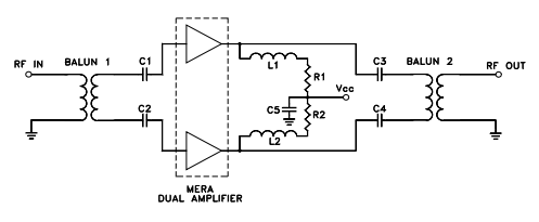
Figure 6 is the schematic diagram of a push-pull amplifier. With suitable choice of the baluns, multi-octave bandwidth can be achieved. The circuit requires few components.
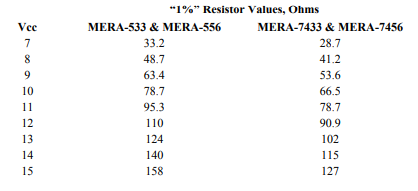
Balun 1 splits the input signal into two amplifying paths that are phased 180 degrees apart. At the output the signals are recombined by Balun 2, so that the fundamental powers add and even harmonics cancel. Separate networks (L1, R1 and L2, R2) apply bias current to the two amplifiers within the package, to isolate the RF paths and ensure constant DC bias. Considerations for design of the bias network for Darlington type MMIC amplifiers are given in Application Note AN-60-010. Optimum bias resistor values for several choices of supply voltage are listed in Table 8.
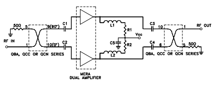
Balanced Amplifier using 90-degree Hybrids
Figure 7 shows the schematic of a balanced amplifier. Very low VSWR is achieved at the input and output, as reflected signals are directed to the 50- ohm terminations via the 90-degree hybrids. The schematic suggests using QBA or QCC or QCN (ultra-small) series Mini-Circuits 2-way 90-degree power splitters/combiners as the hybrids. These hybrids can be used in amplifier designs covering the 300 - 3400 MHz frequency range. Typical balanced amplifier bandwidth when using these 90-degree hybrids is 0.85 times their specified fL-to-fU range.
The bias considerations discussed above regarding push-pull amplifiers apply as well to balanced amplifiers.
Conclusion
The MERA dual amplifiers have been developed to meet the need for closely-matched MMIC amplifiers having high-performance characteristics in a single plastic molded package. In addition to consistent fabrication process control, matching is enhanced by picking adjacent die from the wafer. Thermal management is practical using the techniques described. MERA models are an excellent choice for push-pull and balanced amplifiers.