Transient Protection of Darlington gain block amplifiers
Introduction
Monolithic wideband amplifiers are widely used in the RF and microwave systems. Many of these amplifiers use Darlington configuration. Mini-Circuits monolithic amplifiers with model prefix MAR and ERA, for example, use this configuration. The frequency range of the Darlington amplifiers is specified down to DC, but for proper biasing conditions to occur input and output coupling capacitors need to be incorporated. These capacitors determine the low frequency end of the amplifier frequency range.
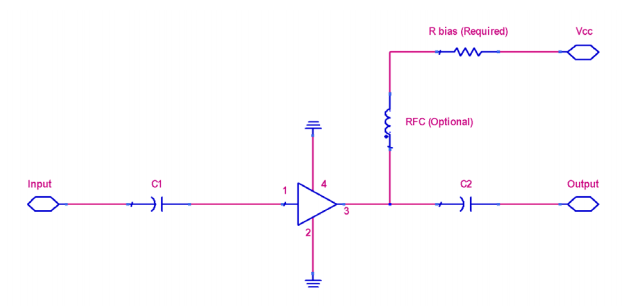
Normally the Darlington gain block amplifiers are designed to operate with an ideal current source. In practice the current source is often substituted with a voltage source and a series resistor, which converts it to a reasonably good current source. The resistor value might be few hundred ohms; therefore, the DC voltage required to operate the amplifier will be higher than the device voltage and may go up to 10 or 15V. An optional RF choke may be connected in series with the resistor to increase the total shunting impedance in order to minimize gain and power loss. The typical biasing configuration is shown in Fig. 1.
During the turn on of the DC supply voltage (Vcc), voltage transients will occur. These transients may damage the amplifier. A new protection circuit is designed (patent pending) to prevent it. This article explains the phenomena and describes the performance of the new amplifiers.
Transient phenomena in Darlington gain block amplifiers
Let's review a simplified schematic (Fig. 2) of a Darlington gain block amplifier with typical bias circuitry.
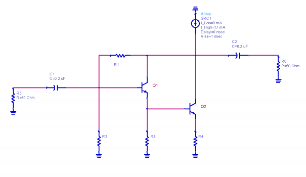
Q1, Q2 are the transistors in Darlington configuration. Resistors R1 through R4 set the bias conditions. C1 and C2 perform a coupling or DC blocking function. R5 and R6 are source and load impedances. The low end of the frequency response dictates that the coupling capacitor values (C1 and C2). The lower the low frequency end, the larger the capacitor values. For example, if the low frequency end of the frequency range is around 100 kHz, the de-coupling capacitors value may be around 0.2 𝓊F. Because the input and output impedance is the same, 50 ohms, normally both input and output capacitors are of the same value.
Let's review that transient process when the current source has sharp ramp (small rise time). The worst case is when the current source jumps from zero to the nominal current value instantaneously. This can happen if we apply the current source by plugging into a connector manually or apply the current by turning a mechanical switch on. At the first moment of turn on, both coupling capacitors C1 and C2 are not charged, and both transistors Q1 and Q2 are not conducting. Let's analyze a simplified circuit (See Fig. 3), the circuit without the transistors Q1 and Q2. It has three ammeters to measure the transient current in the different parts of the circuit. The simulation was performed using ADS 2001 from Agilent.
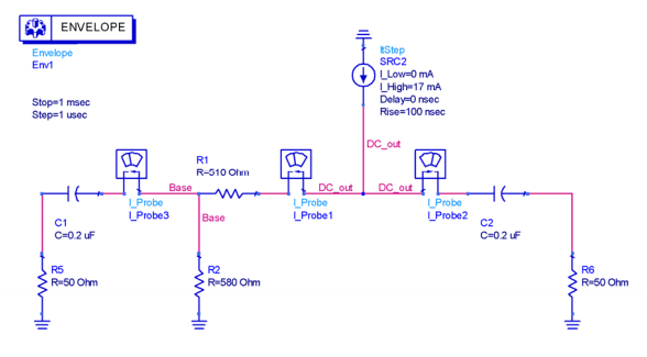
During turn on, the current source starts to charge the capacitors C1 and C2, with different rates due to the difference in time constants (as series resistors are different). The total initial current will be split in the two unequal paths in a proportion approximately (R1+R5)/R6, where R5=50 ohm, R6=50 ohm, R1 may be around 500 ohm, and R2 >> R5.
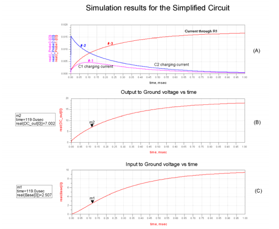
Initially, the current charging capacitor C1 (magenta curve #-1 on Fig. 4(A)) will be 10 times less than the current charging capacitor C2 (blue curve #-2 on Fig. 4(A)). During charging, the current flowing through the capacitors will change because of the current that sinks through R1 and R2 directly to the ground. Once the capacitors C1 and C2 are charged fully, the charge current drops to almost zero (magenta curve #-1 and blue curve #-2 on Fig. 4(A)), Now all the current, 17 mA will sink through resistors R1 and R2. The total voltage drop on the resistors R1 and R2 will reach Icc*(R1+R2)=18.53V (Fig. 4(B)) and this is much higher than the maximum "device voltage". The voltage drop on the resistor R2 will reach Icc*R2=9.86V (Fig. 4(C)) and this is equivalent to the maximum "input" or "base" voltage.
Of course, the voltage will never go this high in the presence of transistors Q1 and Q2. The transistors start to conduct when the voltage drop on resistor R2 reaches approximately 2.6 to 2.8V (twice the Vbe for the InGaP HBT). That will happen at about 119𝓊s. But, the device voltage at that moment is already 7V. When the transistors start to conduct not only the current source pumps in the nominal current Icc=17mA, but the charged output capacitor C2 starts to discharge through the amplifier increasing the stress on the output transistor of the amplifier. The instantaneous power represented by the product of that increased device current and the increased device voltage may have a killing effect on the amplifier. After the first overshoot, conducting transistors are supposed to sink the charge of the capacitor C2, and (if transistors survive) the device voltage settles to a steady 5V.
Now let's analyze the entire amplifier circuit including both transistors Q1 and Q2. Fig. 5 is a transient simulation result using ADS2001 from Agilent.
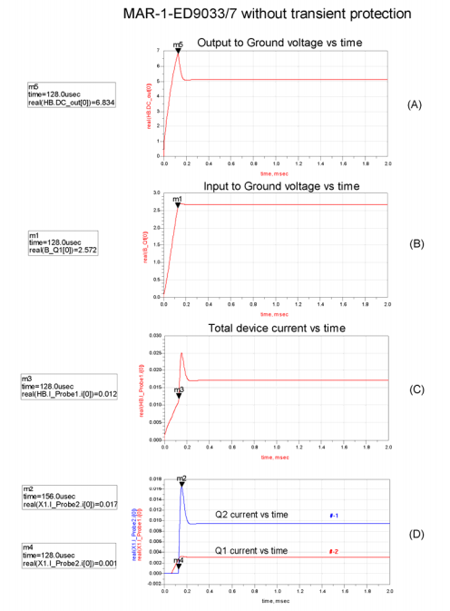
The amplifier output voltage vs. time is shown on the Fig. 5(A). The amplifier input voltage or the base voltage on the transistor Q1 vs. time is shown in Fig. 5(B).
The total current through the amplifier is shown in Fig. 5(C). It includes the current from the current source plus the discharge current from the output capacitor C2. Emitter currents trough transistor Q2 (blue curve #-1) and Q1 (red curve #-2) are shown in Fig. 5(D).
The most dangerous moment is when the total device voltage reaches its maximum value (marker m5 on Fig. 5(A)) and transistor Q2 starts to conduct (marker m4 in Fig. 5(D)). The total device voltage is about 6.83V at this moment. It may cause irreversible breakdown.
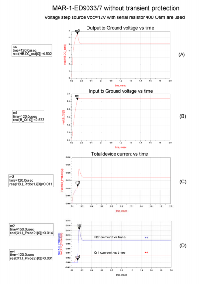
Peak voltage on the output of the amplifier does not exceed 6.5V (see Fig. 6(A)). It is less than the peak voltage of about 6.83V that occurs when using a current source (see Fig. 5(A)). Besides, the peak current through the output transistor Q2 is about 14mA (blue curve #-1 in Fig. 6(C)). It is also less than the peak current of about 17mA through the transistor Q2 in the case of current source (blue curve #-1 in Fig. 5(C)). Therefore, the stress on the amplifier fed with the voltage source and 400 ohm serial resistor is less than from the ideal current source at nominal current. The drawback is weaker RF performance because of finite impedance in the power supply branch.
Actual measurements of the real amplifiers
Fig. 6 and Fig. 7 are the actual measurements of device voltage vs time at different current source values for MAR-1 amplifier without the protective circuit. MAR-1 amplifier is supposed to operate at nominal current of 17 mA. Keithley 236 power supply was used as a current source and Infiniium HP54835A oscilloscope from Agilent was used to capture the device voltage.
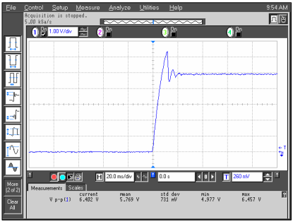
When current step of 14 mA (less than nominal 17 mA) is applied, the peak voltage reaches the value of about 6.4V. The amplifier is able to withstand this stress, and after the transient process is over the voltage stabilizes at a steady nominal value of about 4.9V.
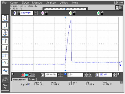
Now, current is increased just by 1 mA. When a current step of 15 mA (still less than nominal 17 mA) is applied, the peak voltage reaches the value of about 6.56V. This exceeds the limit the amplifier can withstand. The amplifier is damaged. After breakdown the voltage stabilizes at steady value of about 0.25V. Fig 8 shows that MAR-1 amplifier without the protective circuit cannot stand the sharp current step with less than nominal value of 17mA.
Another example is amplifier ERA-5. The nominal current for this amplifier is 65 mA. The transient test screenshots for the standard model without transient protection circuit are provided below (Fig. 9, Fig. 10):
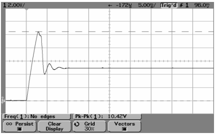
This amplifier is able to stand the current step with its nominal value of 65mA. The peak voltage reaches high 10.42V. But let's see; do we have any margins for the current?
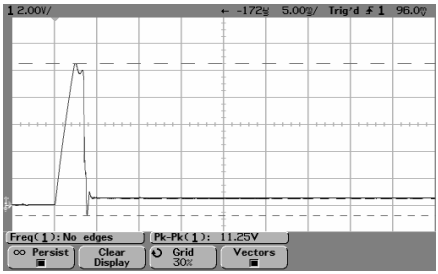
With the higher current step of 75mA the peak voltage reaches the value of 10.5V. That is only 80mV above the peak voltage in Fig. 8. And amplifier does not survive it. After breakdown the device voltage stabilizes at about 0.4V. This is not a robust design.
It is very important to remember that any standard Darlington amplifier has the transient overshoot problem if:
- the rise time of the power supply (current or voltage source) is small, that is, if it is much less than transient process itself, or
- the switch-on time is faster than the longest period of the signal that the amplifier can handle.
If the current source is "slow", such as HP E3631A, there should not be any problem with the transient overshoot. For example, if current is applied "slowly" MAR-1 can work at up to 40mA total current. Therefore, this is not an issue of steady state power dissipation limit.
How to avoid the problem
1. The easiest method is to use a "slow" power supply, or use a slowing (integrating) RC or RLC circuit
2. The second easy way is to reduce the value of the input de-coupling capacitor C1 (to make its charging faster), or (if the low frequency end is critical) increase the value of the output decoupling capacitor C2 (to make its charging slower with respect to the input capacitor). If the C2 value is 5 to 10 times greater than the C1 value, damage due to transient overshoot should not occur The methods described above are good for any existing model of the Darlington gain block amplifier. But for the ultimate protection there is the better way!
3. Mini-Circuits started to design new amplifiers with the special transient protective circuit (patent pending). That protective circuit serves in two ways:
- Prevents voltage overshoot effect during start-up time
- Protects output stage of the amplifier from RF overload if the amplifier is driven significantly above its compression point
The new transient protection circuit does not degrade normal RF performance of the amplifiers and improves the overall robustness and durability of the amplifier.
As an illustration the transient processes of the protected version of the ERA-5-ED9351/8_1 amplifier shown below (Fig. 11, Fig. 12):
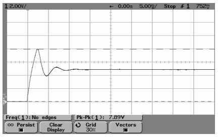
At nominal device current 65mA the peak voltage is only about 7.9V. This is much lower than the peak voltage of about 10.42V for the conventional (unprotected) amplifier (see Fig. 9). After transient process is over the device voltage comes to the steady value of about 4.9V. Of course, the protected amplifier survives.
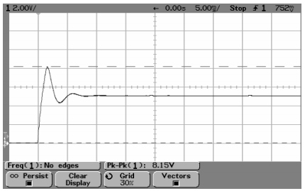
Fig. 11 and Fig. 12 show that the new ERA-5-ED9351/8_1 with protection circuit not only survived at much higher than the nominal current surge (Icc=100mA). For ERA-5-ED9351/8_1 the peak voltage on the output of the amplifier is only 0.25V higher when the current rises from nominal 65 mA to high 100 mA. The peak voltage even at the increased 100mA device current is only 8.15V. This is much lower than the destructive 10.5V in Fig. 9. After the transient process is over the device voltage comes to the same steady value of about 4.9V. The design is robust!
Conclusion:
1. Transient analysis revealed the dangerous start-up overstress, which can cause permanent damage of the conventional Darlington gain block amplifier.
2. Recommendations are given on how reduce the overstress in existing schematic configurations by changing the input or output de-coupling capacitor values.
3. Most effective protection is provided by the newly developed monolithic amplifiers (patent pending) which can withstand much higher stress conditions during start-up and have additional protection from RF overload of the output stage during steady mode of operation. Transient protection circuit greatly improves ruggedness of new amplifiers!
Mikhail Mordkovich, April 7, 2003