Amplifier Terms Defined
1 dB compression point defines the output level at which the amplifier's gain is 1 dB less than the small signal gain, or is compressed by 1 dB (P1dB).
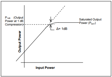
NOTE: Most amplifiers start to compress approximately 5 to 10 dB below P1dB. Applying signal power levels above this point results in a decrease in Gain – therefore, the change in output power will not be linear with respect to a corresponding change in input power to the point where the amplifier is at saturation (PSAT) and the gain equals zero.
Operating at output levels above P1dB is not a normal operation for a linear amplifier.
Conditionally stable amplifier refers to an amplifier which will oscillate under particular load or source impedance (VSWR) conditions, an undesirable situation. (See also Unconditionally stable.)
Cp (Process capability) Process capability is broadly defined as the specification width (S) divided by the process width (P) and is an indication of the spread of the process. Specification width "S" is the difference between the upper specification limit (USL) and the lower specification limit (LSL). Assuming the process to be Gaussian, its standard deviation can be denoted by sigma (σ).
Process width is defined as 6 times sigma (3 sigma on each side of the mean). For example, if the USL and LSL of noise figure of an amplifier are 6.9 and 6.0 dB, then S is 0.9 dB. If the standard deviation is 0.1 dB, then P is 0.6 dB. Cp, the process capability, is 0.9/0.6 = 1.5
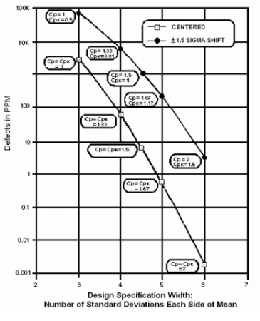
When Cp is 1, then 99.73% of the units pass specs and the process produces 0.27%. defective units. When the value of Cp increases, the number of defects decreases dramatically. Percentage defects is no longer a convenient measure at higher values of Cp; instead, parts per million (PPM) is used to describe the defect rate. For example, when Cp is 1.5, defects are 5 PPM and when Cp is 2 the defects are 0.002 PPM. In this last example (Cp = 2), process width is ± 6σ and the process is called a 6σ process.
All the above numbers are based on the assumption that the center of the spec limits and the center of the process are the same. When this not true, Cp does not provide complete information.
Cpk (Process capability of a non-centered process). Cp does not take into account non-centering of the process and therefore is of minimal value in practice. In the general case a quantity called Cpk is used, which takes into account any non-centering of the process. Two equivalent definitions of Cpk:
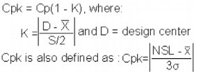
In the Cpk definition NSL is the nearest spec limit, x-bar is the mean of the process, and the vertical lines (denoting absolute value) indicate that Cpk is always a positive number. Cp and Cpk are equal for a centered process. Cpk is also useful for defining processes with single-sided specifications. For example, noise figure of an amplifier has only an upper spec limit and active directivity has only a lower spec limit. In deriving Cpk, one should make sure that x-bar has a meaningful value, such as its being between spec limits when both spec limits are present. For singlesided specs, x-bar should be below the upper spec limit or above the lower spec limit. The graph at the side shows the number of defectives for various values of Cpk.
Directivity (active directivity) is defined as the difference between isolation and forward gain in dB. It is an indication of the isolation of the source from the load, or how much the load impedance affects the input impedance and the source impedance affects the output impedance. The higher the active directivity (in dB), the better the isolation.
Dynamic range is the power range over which an amplifier provides useful linear operation, with the lower limit dependent on the noise figure and the upper level a function of the 1 dB compression point.
Gain flatness indicates the variation of an amplifier's gain characteristic over the full frequency response range at a given temperature expressed in ±dB. The value is obtained by taking the difference between maximum and minimum gain, and dividing it by 2.
Gain (forward gain, G) for RF amplifiers is the ratio of output power to input power, specified in the small-signal linear gain region, with a signal applied at the input. Gain in dB is defined as G (dB) = 10 log10G.
Harmonic distortion is produced by non-linearity in the amplifier, and appears in the form of output signal frequencies at integral multiples of the input signal frequency. Because harmonic distortion is influenced by input power level it is generally specified in terms of the relative level for the harmonics to the fundamental signal power.
Isolation is the ratio of the power applied to the output of the amplifier to the resulting power measured at the input of the amplifier.
Linearity of an amplifier signifies how well its output power can be represented by a linear function of the input power. A linear amplifier produces at its output an amplified replica of the input signal with negligible generation of harmonic or intermodulation distortion.
Maximum signal level refers to the largest CW or pulse RF signal that can be safely applied to an amplifier's input. Exceeding the specified limit can result in permanent noise figure degradation, increased distortion, gain reduction, and/or amplifier burnout.
Noise factor is the ratio of signal-to-noise power ratio at an amplifier's input to the signal-to-noise power ratio at the output. Noise figure NF in dB is related to noise factor F by NF = 10 log10F in dB.
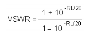
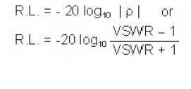
Return loss (RL) is the ratio of reflected power to incident power at an RF port of an amplifier, expressed in dB as RL = -20 log |ρ|, where ρ = voltage reflection coefficient.
Reverse gain is the ratio of power measured at the input of an amplifier to the applied power at the output of an amplifier, also known as isolation.
Sigma is the statistical term for the Standard Deviation of a distribution. All nominally identical things differ one from another to a greater or lesser degree. Standard deviation is a measure of how much a distribution varies around the average (mean) value. Many distributions when plotted have a bell-shaped appearance, and are characterized as a normal distribution.
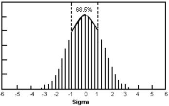
The standard deviation is the distance from the center of a normal distribution curve to where the curve changes direction (its point of inflection), and is denoted by the Greek letter sigma (σ).
Sigma performance, SP, tells how far the nearest spec limit is from the average, compared with the sigma value. For example, if the spec limit is 6 sigma away, the process has SP = 6. Thus, SP equals 3 times the Cpk value.
"Skinny" sigma refers to a process having small standard deviation and process width (the width at ± 3σ) relative to the specification limits. It reflects a favorable relationship between the process width and the width of the specification. For example, in a well controlled process the deviation from one unit to the next is small, and most units fall well within the spec limits. Narrow variation indicates "skinny" sigma. In a process that is not tightly controlled, units will vary from one spec extreme to the other or even exceed the spec limits; in that case the process width and sigma are wide. What causes some confusion is the fact that 6 sigma is skinny while 2 sigma is wide; 6 sigma means the spec limits are much further away from the distribution.
Stability of an amplifier is an indication of how immune it is to self-oscillation, so that it does not generate a signal at its output without an applied input. A commonly used indicator of stability is the k-factor. A k-factor of 1.0 is the boundary condition for unconditional stability. If it is greater than zero but less than 1.0 the amplifier is only conditionally stable.
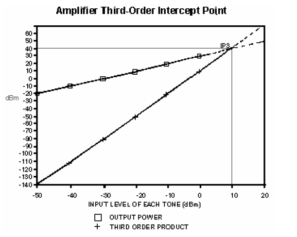
Two-Tone Third-order intercept point is a measure of third-order products generated by two equal-amplitude signals arriving simultaneously at the input of a device such as an amplifier. If F1 and F2 are the frequencies of the two signals arriving at the input, the amplifier generates intermodulation products at its output due to inherent non-linearity, in the form ± m × F1 ± n × F2 where m and n are positive integers which can assume any value from 1 to infinity. The order of the intermodulation product is defined as m + n. Thus, for example, 2 × F1 – F2, 2 × F2 – F1, 3 × F1 and 3 × F2 are third-order products by definition. The first two products are called two-tone third-order products as they are generated when two tones are applied simultaneously at the input. The latter two are single-tone third-order products, usually called third-harmonic products.
For example, if 100 and 101 MHz are the frequencies of two applied signals, then 99 and 102 MHz are the two-tone third-order products and 300 and 303 MHz are singletone third-order products. Two-tone third-order products are very close to the desired signals and are very difficult to filter out. Hence they are of great importance in system design. In the linear region, third-order products decrease/increase by 3 dB for every 1 dB decrease/increase of input power, while the desired output signal power decreases/increases by 1 dB for every dB of input power.
When drawn on an X-Y graph with input power on the X-axis and output power on the Y-axis, third-order products fall on a straight line with a slope of 3 while the desired (fundamental) signal power falls on a straight line with a slope 1 as shown below. By extending the linear portions the two lines, they intercept at a point. The X co-ordinate and the Y co-ordinate of this point are called the input and output third-order intercept point respectively, and the two differ by an amount equal to the small-signal gain of the amplifier. In the example shown, small-signal gain is 30dB and output IP3 is 40dBm.
Output intercept point, IP3 (dBm)out, can be calculated using a simple formula:
IP3 (dBm)out = Pout (dBm) + A/2
where Pout (dBm) is the output power of each tone in dBm and "A" is the dB difference between the per-tone output power and the intermodulation power. Input intercept point is obtained by substituting Pin (dBm) for Pout (dBm) in the above formula. Single-tone and two-tone third-order intercept points differ by a fixed amount on the Y-axis, but the output/input lines have the same slope.
Unconditionally stable refers to an amplifier that will not oscillate regardless of load or source impedance.
VSWR (voltage standing wave ratio) is related to return loss (RL) by the following:
Two Dozen Often-Asked Questions About Amplifiers
I. Q. What is the effect of using a 50-ohm amplifier in a 75-ohm system?
A. When a 75-ohm load is seen from an ideal 50-ohm amplifier or vice-versa, a 1.5:1 VSWR results which alters gain, output return loss, and gain flatness in real-life amplifiers. If active directivity (defined as isolation minus gain) is low, a change in load impedance will result in a change of input impedance and a change in source impedance will result in a change in output impedance. Hence, a 75-ohm load on an amplifier with low directivity will affect the input impedance of an amplifier. Maximum transfer of power may not occur. However, in many applications, the mismatch may not be objectionable. For specific performance details, the 50-ohm amplifier should be tested under 75-ohm conditions.
II. Q. What is output VSWR and what is its significance?
A. Output VSWR is a measure of how much power is reflected back from the amplifier's output port when an external signal is applied to that port. VSWR varies from a theoretical value of 1:1 for a perfect match to greater than 20:1 for total mismatch. Since loads in practical applications vary with frequency, maximum power and gain flatness also will deviate from what is specified. If the amplifier is connected to its load by a cable and all three have different impedance, then multiple reflections between the amplifier and its load can occur resulting in greater variation in frequency response. In general, the output impedance (characterized by output VSWR) is the source impedance of the following device.
III. Q. How is output VSWR measured?
A. A simple setup using a directional coupler is shown below.
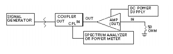
First establish the 0-dB reference as follows. Apply the input signal to the directional coupler output port as shown. Apply a short circuit to the coupler's input port and measure the power at the coupled port. Then replace the short with an open circuit and note the reading at the coupled port. The average of the two readings is the 0-dB reference. Next substitute the open circuit with a 50-ohm load. Note the reading; this will give you the measurement range of the setup. Remove the 50-ohm load and replace it with the DUT. Measure how far the reflected signal is from the 0-dB reference; this is the output return loss (RL). To convert output return loss to VSWR, use the formula: For more accurate measurements, use a vector network analyzer.
IV. Q. What is the relationship between reflection coefficient, VSWR, and output return loss?
A. The voltage reflection coefficient (ρ) is the ratio of the reflected to incident voltage in an amplifier or device. The theoretical reflection coefficient varies from zero for a perfect match to one for a total mismatch. Magnitude of reflection coefficient and VSWR are related by
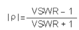
Return loss is related to the magnitude of reflection coefficient |ρ| by
V. Q. To improve matching, can I use a resistive pad between amplifier stages?
A. Of course. But at the expense of overall gain, noise figure, and/or output power. The higher the gain of the first stage and the lower the value of the attenuator, the less the degradation of noise figure. Overall noise factor is calculated as follows:
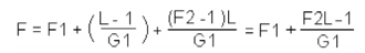
where F1, F2 are noise factors of first, and second amplifiers, and L is the loss factor of the pad.
Noise figure in dB = 10 log10F, where F is noise factor
Loss in dB = 10 log10L, where L is loss factor
Gain in dB = 10 log10G, where G is gain factor
VI. Q. What is the significance of an amplifier's directivity characteristic in a system design?
A. Directivity is the difference between isolation and gain. Directivity is an indication of how the impedance mismatch at the amplifier's output affects the input.
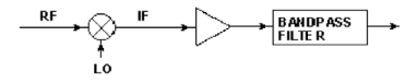
In receiver applications, a filter following a wide-band amplifier rejects high-frequency spectral components generated by the mixer, by reflecting them back to the amplifier. If the amplifier has poor directivity, the reflected components will reach the mixer and could affect mixer performance adversely.
If the amplifier provides high directivity, the reflected signals reaching the mixer will be much lower in magnitude and thus cause little interaction at the mixer stage.
Another common application is two-tone, third-order IM testing, where the two-tone signals must be well isolated; amplifiers with high directivity are used between source and combiner.
For relatively high RF frequencies, isolators can be used but they are expensive; for frequencies below 1 GHz, they are difficult to find. High-directivity amplifiers, such as Mini-Circuits' MAN-AD series, are recommended for such applications.
VII. Q. Can I obtain higher power output by paralleling amplifiers?
A. Yes, but it's not as simple as merely connecting the two inputs and the two outputs in parallel. It involves judicious use of power hybrids with proper amplitude and phase balance and power levels, as well as amplifiers well matched for gain and phase characteristics. Examples are the HELA-10 and MERA series of amplifiers.
VIII. Q. I want to vary an amplifier's gain. Can I adjust the amplifier's supply voltage to achieve an AGC effect?
A. It's not recommended. An amplifier is designed to operate at a given supply voltage and its performance specifications (gain, power output, saturation, frequency response, etc.) are based on the stated supply voltage. Boost the supply voltage too much and gamble on the amplifier burning up; reduce the supply voltage too low and expect the performance specs to deviate considerably.
A voltage-variable attenuator such as ZX73-2500 can be used with the amplifier to vary the overall gain.
IX. Q. I'm working with a 12-volt system and am considering your +30 dBm ZHLseries amplifiers such as ZHL-42. The specs indicate a +15 volt supply is required. How will performance be affected with 12-rather than 15-volt DC input?
A. Typical performance data are available on the Mini-Circuits website for many amplifier models at three DC power supply voltages, such as +12, +15, and +16, volts.
XI. Q. My application involved injecting sharp RF pulses to an amplifier. How can I tell whether the amplifier's peak power limits will be exceeded?
A. Here's a conservative rule-of-thumb estimate for a 50-ohm amplifier. (1) Take the amplifier's maximum input power rating. (2) Convert from dBm to W. (3) Multiply by 100. (4) Take the square root, and use this figure as the maximum peak signal in volts that can be applied.
XII. Q. When an amplifier is used in a test setup, is there such a thing as a safe sequence to connect the amplifier's input, output, and supply voltage to avoid damage?
A. Yes, there is a recommended procedure. Begin by connecting the load, then the DC supply, and finally the RF input signal. When finished, first disconnect the RF input, then the DC power, and finally the load.
XIII. Q. Please sketch the test setup and describe the test procedure used to measure an amplifier's second-order intercept point.
A. Block diagram of a set up for measuring amplifier two-tone distortion is shown below. The product F1 + F2 of an amplifier is quantified and specified in terms of its second order intercept point (IP2). In the linear region of the amplifier, if second harmonic is A2 dB below fundamental, this IP2 is given by
IP2 (dBm) = Pout (dBm) + A2
In the block diagram, a low-pass filter is provided to attenuate second harmonics of the generator 10 to 20 dB below that generated by the device under test (DUT). Sufficient attenuation should be provided at the DUT output to prevent spectrum analyzer from generating harmonics.
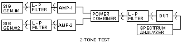
XIV. Q. Describe the procedure for measuring 2-tone 3-order intercept point of an amplifier.
A. Block diagram of a setup for measuring two-tone third-order intercept point is shown above.
If F1 & F2 are the frequencies of the two tones, then 2F1 – F2 and 2F2 – F1 are the third-order products. The setup should ensure that second harmonic of F1 & F2 are at least 10 to 20 dB below the third-order products to be measured. Care also should be taken to prevent F1 & F2 interaction and generation of third-order products in the instrumentation. Amplifiers 1 and 2 are selected such that they have high directivity. This provides the desired isolation of the generators. If POUT is the desired signal, and A3 is the level of the third-order product below the desired signal, then the output third-order intercept point is given as
IP3 (dBm) = POUT (dBm) + A3 ÷ 2
Example: Let Pout = +10 dBm, and let the 2-tone third-order products each be – 30 dBm (40 dB below POUT). Then, IP3 = +10 + 40 ÷ 2 = +30 dBm.
XV. Q. Does the Gain spec of a MMIC amplifier such as ERA-2SM+ have to be adjusted by 6 dB to account for the 50-ohm source and 50-ohm load impedances?
A. No, "Gain" is actually Insertion Gain, which is the dB-increase in output power observed when the amplifier is inserted between the 50-ohm source and 50-ohm load.
XVI. Q. Please explain the specifications in Amplifier data sheets headed "Maximum Power Output".
A. The quantity under the sub-heading "(1-dB Compr.) Min." is the minimum value of output power at 1-dB gain-compression (P1dB).
Most amplifiers start to compress approximately 5 to 10 dB below P1dB. Applying signal power levels above this point results in a decrease in Gain; therefore, the change in output power will not be linear with respect to a corresponding change in input power to the point where the amplifier is at saturation (PSAT) and the gain equals zero. Operating at output levels above P1dB is not a normal operation for a linear amplifier.
The quantity under the sub-heading “Input (no damage)” is the value that must not be exceeded at any time; if that power is actually applied, the amplifier will be in saturation.
XVII. Q. What is the maximum operating value of junction temperature for MMIC Darlington amplifiers, such as ERA or GVA series?
A. The maximum operating value can be found as follows:
1) From the Data Sheet of the desired model, calculate power dissipation as the product of "Recommended Device Operating Current" (Max. value of "Device Operating Current" for GVA) and Max. value of "Device Operating Voltage".
2) Calculate junction-to-case temperature rise as the product of that power and "Thermal Resistance, junction-to-case".
3) Calculate the junction temperature as the sum of (a) that temperature rise, (b) 85 degrees C, and (c) the temperature-rise-above-ambient value given in the note next to the Absolute Maximum Ratings table.
Example, for GVA-84+: 0.13A x 5.2V x 64C/W + 85 + 10 (typical temperature rise due to the thermal resistance of the user’s PC board to ambient) = 138C.
XVIII. Q. Can the monolithic Darlington amplifiers such as the ERA, Gali, GVA, MAR and MERA series be operated at low RF frequencies down to DC?
A. These MMIC Darlington amplifiers can be used at as low a frequency as desired, by user's choice of blocking capacitors. However, they cannot be DC-coupled. The reason is that they generate internally a DC bias voltage at the input terminal, which would be upset by using DC coupling.
XIX. Q. MMIC amplifier data sheets give a typical value for thermal resistance junction-to-case. How can I determine thermal resistance junction-to-air, in still-air condition?
A. The process is given below, using Model Gali-74+ as an example. The data sheet on the Mini-Circuits website for that model has a typical value for thermal resistance junction-to case: 120 degrees C per watt. A note under the Absolute Maximum Ratings table in the data sheet states that operating temperature is based on typical case temperature rise 6 degrees above ambient. That is for PC boards commonly used for this type of component, in still air condition. Given the typical Gali-74+ power dissipation, 0.080 ampere × 4.8 volts = 0.384 watts, we can estimate the thermal resistance from the case to ambient as 6 degrees / 0.384 watts = 15.6 degrees C per watt. Therefore, thermal resistance junction-to-ambient is the sum of these values: 120 + 15.6 = 136 degrees C per watt.
XX. Q. For worst-case MMIC amplifier junction-temperature calculation should the absolute maximum values of operating current and input power be used?
A. No, because the absolute maximum values of current and input power in the data sheet are never to be exceeded and are not intended for continuous service. Use the "recommended device operating current" and the maximum specified "device operating voltage" to calculate worst-case power and junction temperature. RF output power, especially when operating at or near the amplifier’s 1-dB gain compression point, can be a significant fraction of the DC power. Because the RF output power is delivered to an external load instead of being dissipated as heat, it can be subtracted from the DC power when calculating the junction temperature. (This effect is known as “RF cooling” of the amplifier.)
XXI. Q. Why do some amplifiers such as ZX60-14012L+ have multiple operating temperature ratings, case and ambient?
A. The user can work with either the case temperature rating or the ambient rating for such an amplifier, as they are equivalent. An amplifier dissipates a significant portion of its DC input power as heat, causing the case temperature to rise above ambient air. The higher the DC voltage among the rated values, the higher is the case temperature rise at the same ambient temperature. To keep the case temperature within reliability goals, the maximum ambient rating is reduced at higher DC voltage.
XXII. Q. ZRL- series amplifiers have dual temperature ratings, ambient and case. Do these amplifiers need a heat sink?
A. Operating temperature range of ZRL- series amplifiers is rated at -40 to 60 degrees C ambient, and -40 to 80 degrees C case. A heat sink is not required if ambient air does not exceed 60 degrees C. Above that temperature, a heat sink or forced-air cooling should be used so that the case temperature does not exceed 80 degrees C.
XXIII. Q. Some amplifiers such as ZHL-20W-13 are offered with and without the heat sink. If I buy it without the heat sink (such as ZHL-20W-13X), what external heat-sinking do I have to provide?
A. A note on the data sheet tells the user the maximum base-plate temperature for the X-suffix model, and states the thermal resistance required via the user's external heat sink. Using ZHL-20W-13X as an example, a heat sink with thermal resistance of 0.3 degrees C per watt is needed to limit the base-plate to 85C in a 65C ambient environment. The temperature rise with such a heat sink is 20 degrees C. Suppose your actual maximum ambient is lower, say 50 degrees C. Then, the 85 degrees maximum base-plate temperature still applies, but the 35-degree rise above your maximum ambient allows you to use a heat sink with worse (greater) thermal resistance: 0.3 X 35/20 = 0.525 degrees C per watt.
XXIV. Q. If I apply DC power to a high-power amplifier such as ZHL-10W-2G+ by increasing the voltage slowly, I notice that when DC current starts to flow it is initially higher than expected, and then it decreases as I continue to increase the voltage to the normal operating value. Is this a fault?
A. It is normal behavior. This kind of amplifier contains a switching voltage regulator that automatically adjusts the current taken from the user's power supply to compensate for change in DC voltage. The result is nearly constant DC power consumption and RF performance. For example, DC current drawn by ZHL-10W-2G+ is typically 4.25A at 21V, 3.7A at 24V, and 3.5A at 26V.