Low Cost Very High IP3 Low Noise Amplifiers Cover 250MHz to 2300MHz
Mini-Circuit’s Blue Cell technology allows the use of its 90-degree splitters to enhance the performance of a family of medium power amplifiers. Balanced amplifier configurations offer several performance advantages when compared to single-ended designs. The foremost advantage is the improvement of both input and output return loss due to reflections canceling in the hybrid couplers. Amplifier design stability is also more predictable due to each active device being terminated in a 50-ohm load. Furthermore, output power and third order intercept performance are twice that of a single device amplifier. Lastly, if one half of a balanced amplifier fails, it will still operate with a gain reduction of about 6 dB.
Balanced Amplifier Operation
Balanced Amplifier Operation Figure 2 shows a block diagram of the balanced amplifier configuration. The amplifier consists of two identical gain stages in each half, preceded by a splitter, and followed by a combiner. The amplifier is specified to operate at 12V DC. Custom voltages in the range of 6.5V to 17V are available on special request.
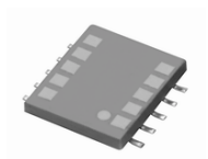
The splitter/combiners are the QBA series of Blue Cell Technology low-temperature co-fired ceramic (LTCC) 2-way 90-degree quadrature hybrids. These low cost LTCC hybrids offer the low insertion loss, excellent phase and amplitude balance that makes a high performance balanced amplifier possible. Figure 3 shows the QBA series of power splitters using LTCC technology.
The input QBA divides and applies the power equally to the two amplifier halves. The output QBA recombines the two output powers from the amplifiers. The input and output reflected signals of A1 and A2 are coupled to the 50-ohm ports of the hybrids. The balanced amplifier input/output port return losses can be predicted using equations:
Input return loss: |S11| = 0.5 |S11a – S11b|
Output return loss: |S22| = 0.5 |S22a – S22b|
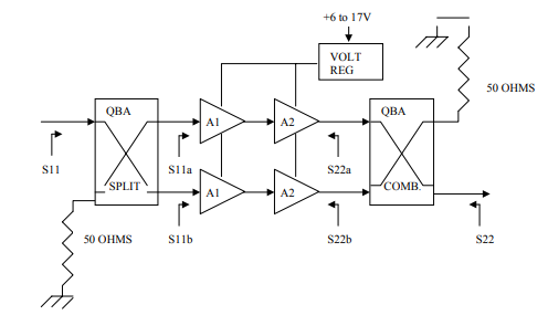
Both input and output port return losses will be dependent upon the matching or balance of the amplifier stages, and the balance of the splitter/combiner
The usable bandwidth of the QBA series of splitters in balanced amplifiers is much greater than the normal published QBA specifications. A QBA-24 splitter has shown a balanced amplifier –1 dB bandwidth of 1.0 to 3.0 GHz during tests.
The two gain stages in each side of the balanced amplifier have been designed to cascade for optimal overall performance. Gain, frequency response, noise figure and third order intercept points are all factors that must be considered when cascading amplifier stages. The design of this family of amplifiers was optimized for high third order intercept performance while maintaining a combination of high dynamic range and wide band width.
The dynamic range of an amplifier may be determined if the –1dB output compression, noise figure, minimum discernable signal (MDS) and gain are known.
Dynamic Range: DR = Pin – MDS
Where Pin is the input power which produces 1dB of output power compression, and MDS is the minimum discernable signal at a given bandwidth. Pin and MDS are determined by:
Pin(dBm) = P-1dBout(dBm) – Gain(dB) + 1dB
P-1dBout is the output power at the –1dB compression point.
Gain is the amplifier gain in dB.
MDS = -111dB/MHz + BW (dB) + NF (dB)
BW is the amplifier bandwidth relative to a 1 MHz bandwidth in dB.
NF is the amplifier input noise figure in dB.
The resultant equation for determining amplifier dynamic range is:
DR = [P-1dBout (dBm) – Gain (dB) + 1dB] – [-111dB/MHz + BW (dB) + NF (dB)]
The dynamic range that an amplifier can utilize before being degraded by spurious signals is a more useful definition in the real world. When more than one signal is applied to an amplifier the ideal dynamic range is degraded by the third order products. The dynamic range that is free of spurs when two equal amplitude signals are applied to the input can be determined if the third order output intercept point, gain and minimum discernable signal level are known.
Spurious Free Dynamic Range = 2/3[OIP (dBm) – Gain (dB) – MDS (dBm)]
OIP is the 3rd order output intercept point in dBm.
Gain is the amplifier gain in dB.
MDS is the minimum discernable signal level in dBm, as described above
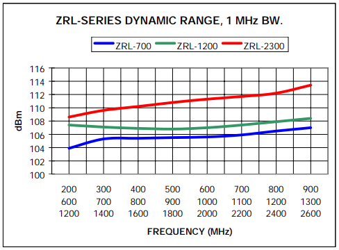
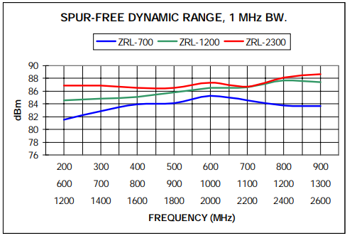
Figures 10 and 11 show the dynamic range and spurious free dynamic range of the ZRL series.
Electrical Performance
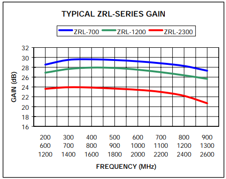
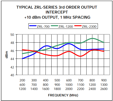
Figure 4 shows the typical frequency responses of this amplifier family. The gain bandwidths at the +/- 1 dB points are 450 to 900 MHz depending upon frequency range. Figure 5 shows the typical 3rd order output intercept points for the three models when tested at +10 dBm single tone output power level. These amplifiers deliver consistently high intercept performance over their pass band and are specified to give intercepts of +44 dBm minimum, +46 dBm typical.
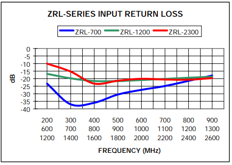
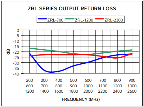
Figures 6 and 7 show the typical input and output return losses. The broad frequency response of the return loss is one of the benefits, and a characteristic of balanced amplifier designs.
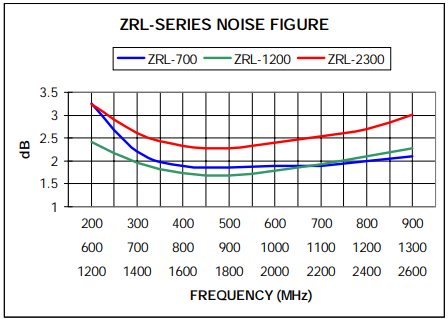
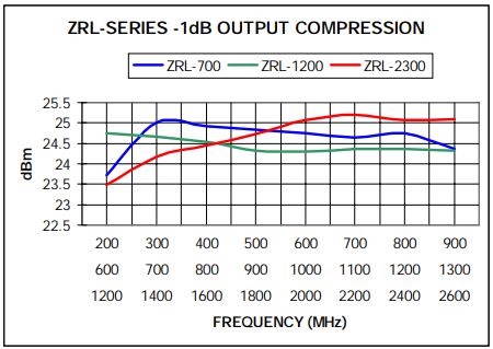
High dynamic range amplifiers need to simultaneously provide low noise performance and high output power. The noise figure and –1 dB output compression performance is shown in Figures 8 and 9. Noise figures in the 2 dB range, coupled with the +25 dBm output compression level results in excellent dynamic range.
Figures 10 and 11 show the ideal dynamic range and the spurious free dynamic range in 1 MHz bandwidths. Determining the spurious free dynamic range at a given output power is one of the better ways to judge the performance of any amplifier. It is dependent upon a combination of parameters that more accurately reflect amplifier performance that is needed in current and future communications.
Balanced Amplifier Construction
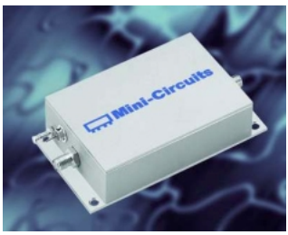
The ZRL family of amplifiers are housed in milled 6061-T6 aluminum housings for structural integrity and heat sinking. The housing is yellow irridite coated to Mil-C-5541 class 3 specifications. SMA connectors are used for the input/output ports with a pin type feed-though capacitor with ground post for the DC input. Six threaded 2-56 holes are available on the bottom of the housing for mounting.
Conclusion
The ZRL family of amplifiers has been designed to provide the high performance needed in the communications industry. Their high output intercept, medium power and low noise, coupled with broadband frequency response, result in a family of medium power amplifiers with excellent overall performance.