UNDERSTANDING NOISE PARAMETER MEASUREMENTS
Overview
This application note reviews noise theory & measurements and S-parameter measurements used to characterize transistors and amplifiers at Modelithics, Inc.
Definitions and Theory
The formulations in this note were derived from multiple sources, including References [1-3]. The noise figure F of a device or component is described by the following relations:
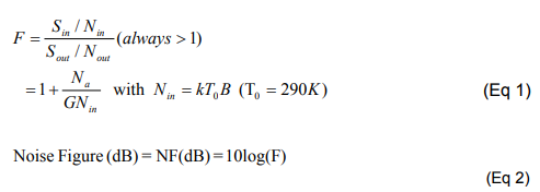
Where Sin,(Nin) and Sout (Nout) are the signal (noise) levels at the input and output of the device, respectively, and Na is the noise added by the device itself, G is the gain of the device, B is the system bandwidth and k is Boltzman's constant (1.38 x 10⁻²³ joule/kelvin). Noise figure is of particular interest to receiver designers as the the minimum detectable signal is dependant on the Noise Figure as follows:

This approximation assumes the background or ambient (= kTB ) noise is that due to a passive device held at T = 290K, and the Required SNRdB represents the minimum signal to noise ratio for acceptable system performance.
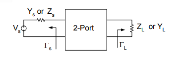
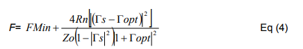
Noise parameters describe how the noise figure varies with source reflection coefficient Γs. Consider Figure 1. There are several formulations for noise figure in terms of noise parameters. One of the popular forms is summarized in (Eq 4).
4 Noise Parameters:
Rn= Equivalent Noise Resistance
FMin= Minimum Noise Figure
|Γopt| : magnitude of optimum noise reflection coefficient
∠Γopt : phase of optimum noise reflection and
Zo = Characteristic impedance (50 Ω)
The above equation provides a description of noise figure in terms of four (4) noise parameters and the source impedance. One common parameter is the minimum noise figure Fmin which will be achieved at some specific optimum (complex) reflection coefficient (Γopt). So in addition to Fmin, two of the other parameters magnitude and angle Γopt, with the fourth parameter being the equivalent noise resistance Rn It should also be noted that there are other noise parameter formulations in addition to those listed in (Eq 4).
One of the common application for noise parameters is for low noise amplifier (LNA) design. Typically a LNA is used at the front end of a receiver to improve the noise figure of the receiver, or essentially boost the signal while adding a low amount of noise to the signal. In addition to its noise figure the gain of the LNA (and correspondingly the transistors used to make up the LNA) is also important. To better understand this, the following equation can be used to calculate the total noise figure of a cascade connection of three different two port devices with gains Gi and noise figure Fi (i= 1, 2, 3).
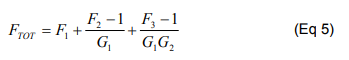
If an LNA with high Gain G1 and low noise figure F1 is the first device then the system noise figure FTOT can remain low even if the second and third devices have a much higher noise figure. The gain used in most noise calculations, including the cascade noise figure equation above is the available gain which can be expressed in terms of S-parameters as follows:
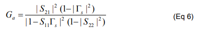
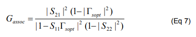
The associated gain assumes that the load port of Fig. 1 is terminated in a conjugate match for a given source reflection coefficient Γs . The associated gain is often tabulated along with noise parameters and is simply the available gain from (Eq 7) for the particular case of Γs = Gsopt.
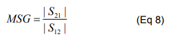
Another set of parameters often plotted are the maximum stable gain, MSG, and maximum available gain, MAG. Often amplifiers or transistors are unconditionally stable over a certain frequency range and conditionally stable at other frequencies.
For frequencies where the device is potentially unstable (with stability factor K < 1), the maximum stable gain is defined as the highest realizable gain with passive terminations, after the device is stabilized with cascaded resistance to border line stability; that is, to bring about the condition K = 1. MSG is given by:
Maximum available gain at frequencies where K>1 (unconditionally stable) is given by:
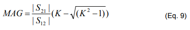
Hence, MSG and MAG numbers in decibels give the amplifier designer a measure of the maximum gain realizable through impedance matching of the amplifier or transistor. Of course the conditions for matching the input for maximum gain and minimum noise figure may be conflicting and a trade-off between these two may be required. While outside the scope of this note, the plotting of noise figure circles and available gain circles can often be used to aid the designer in choosing the best compromise in matching impedance taking noise and gain into consideration (see [2]).
Test Configuration and Calibration
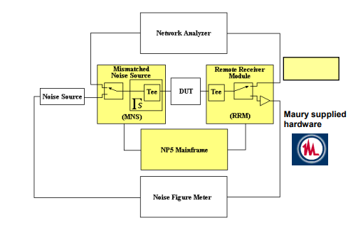
A basic test configuration used to perform combined noise parameter and S-parameter testing is shown in Figure 2. The network analyzer is needed for performing S-parameters of the DUT, which are required for design analysis along with the noise parameters. The network analyzer is also needed to make measurements that are required for calibration of the noise parameter test system.
The test system of Figure 2 is referred to as an "NP5" system and uses a hardware setup and measurement method originally developed by Adamian [5] and commercialized by ATN Microwave. The system consists of a noise figure measurement system (e.g. HP 8971C/HP8970B combination or alternative), a network analyzer (e.g. HP8510C or alternative), a mismatched noise source (MNS), and a remote receiver module (RRM). The MNS and RRM each contain a switch that is used to select either the S-parameter measurement mode or the noise parameter measurement mode. They each also contain a bias Tee for applying bias to the input and output of the device under test (DUT). The MNS is generally a solid-state tuner capable of presenting multiple different values of Γs (see Fig. 1) to the DUT, along with the ability to have a "50 ohm" thru-state that allows the noise source to be connected to the DUT through essentially a transmission line. With the RRM switch in the noise measurement position, the RRM includes a low-noise amplifier in the path to the noise receiver to improve the measurement receiver noise figure.
In the S-parameter measurement mode the system is calibrated using thru-reflect-line (TRL) or alternative high accuracy calibration approaches [6, 7]. To calibrate and operate the noise parameter measurement system, the Maury ATS software [4] is used to perform a series of steps that may be summarized as follows:
- Perform a 2-port S-parameter calibration to establish measurement reference planes at the input and output of the DUT. Store these calibration coefficients in a selected calibration kit file.
- Perform a 1-port short-open-load S-parameter calibration at the position of the noise source, with a thru device connected in place of the DUT. Store these calibration coefficients in a second selected calibration kit file.
- Calculate the S-parameters of the MNS thru path from the noise source to the DUT. The Maury ATS software does this automatically using the calibration information from steps 1 and 2, it also measures the noise source reflection coefficient in the hot/biased on state and the cold/biased off state.
- Perform a tuner characterization. The software uses the calibration information from Step 1 to measure and store hundreds of different Γs values that can be presented at each frequency to the DUT by the MNS during subsequent measurements.
- Perform a noise calibration. With a thru connected in place of the DUT and the system switches set to noise measurement position, the ATS software controls the instruments to record the received noise power for the MNS thru state with the noise source diode biased on and off, and for several different Γs values achieved with the MNS for the case of the diode biased off.
- The ATS software utilizes the information from the previous steps along with the algorithm developed by Adamian [5] to calculate and store the noise parameters of the receiver along with other system information.
- Once calibration is complete, the DUT is connected and the S-parameters and noise parameters of the DUT are measured in sequence (usually S-parameters, then noise parameters). Post processing and noise parameter data smoothing is sometimes needed and is provided for in the Maury ATS software.
Example Results
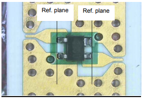
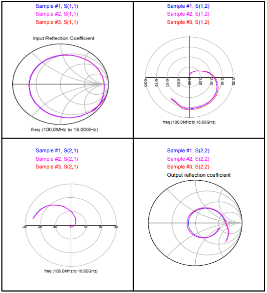
In the following we will use data taken on samples from the Mini-Circuits SAV amplifier series. Figure 3 shows pictures of a device sample as mounted in a coplanar waveguide test fixture setup for RF wafer probe testing. TRL standards, fabricated with the same ground-signalground test interface were used along with the NIST Multical method [6] to establish measurement reference planes at the locations indicated in Fig. 3. These same reference planes were established for noise parameter measurements using the Maury ATS software. Fig. 4 and Fig. 5 show example S-parameter and noise parameter measurement results made on 3 test samples.
References
- G. Vendelen, A. Pavio and U. Rohde, Microwave Circuit Design Using Linear and Nonlinear Techniques, 2nd Ed., John Wiley & Sons 2005.
- Guillermo Gonzalez, Microwave Transistor Amplifiers Analysis and Design, 2nd edition, Prentice Hall, 1997.
- R. Gilmore and Les Besser, "Practical RF Circuit Design for Modern Wireless Systems", Volume II: Active circuits and subsystems, Artech House, 2003.
- Maury Microwave Corporation, 2900 Inland Empire Blvd. Ontario, California 91764 USA. www.maurymw.com
- V. Adamian and A. Uhlir, "A Novel Procedure for Receiver Noise Characterization," IEEE Trans. on Instr. And Meas., June 1973.
- R. Marks, "A multiline method of network analyzer calibration,"IEEE Trans. Microw. Theory Tech., vol. 39, no. 7, pp. 1205-1215, Jul. 1991.
- S. Padmanabhan et. Al, "Broadband space conservative on-wafer network analyzer calibrations with more complex load and thru models,"IEEE Trans. Microw. Theory Tech., vol. 54, no. 9, pp3583-3592.
About this note
This note was assembled as a collaboration between Mini-Circuits and Modelithics, Inc. with information and assistance provided by Maury Microwave (www.maurymw.com).
Contact information
For information about Mini-Circuits products and support, please contact Mini-Circuits at P.O. Box 350166, Brooklyn, NY 11235 U.S.A. voice: 718-934-4500 fax: 718-934-7092 web www.minicircuits.com
For information about Modelithics products and services, please contact Modelithics, Inc. , 3650 Spectrum Blvd. , Suite 170, Tampa, FL 33612. voice: 888- 359-6539, fax: 813-558-1102, email sales@modelithics.com , web www.modelithics.com