Semiconductor Die Ordering and Packaging Information
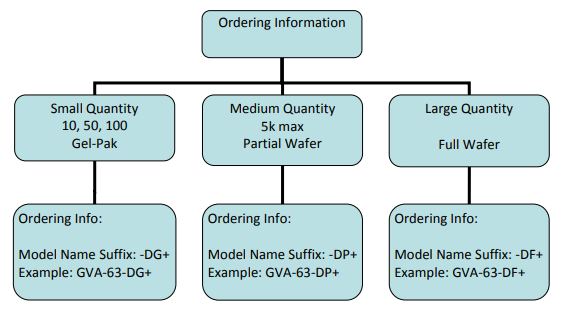
Ordering Information
Mini-Circuits markets Semiconductor Die as a standard Catalog Product. Based on the quantity requirement of the customer, die is shipped in:
- Gel-Pak for small quantities; 10, 50, 100 KGD1
- Partial Wafer; quantity <5k KGD1
- Full Wafer KGD1, 2
Above are typical of small die. Please refer to Die Data Sheet for model specific quantities.
Packaging Information:
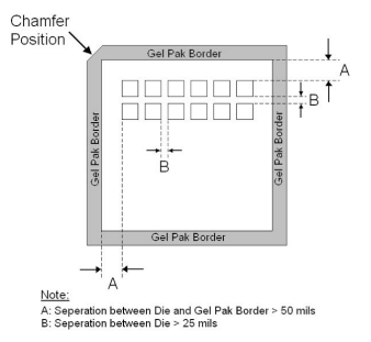
Gel-Pak Packaging (For Small Quantity)
Partial Wafer (For Medium Quantity)
Sorted dice array contains DC-tested and passed units. A 2.5" x 2.5" array of sorted dice is mounted on membrane in the center of a metal ring without expansion.
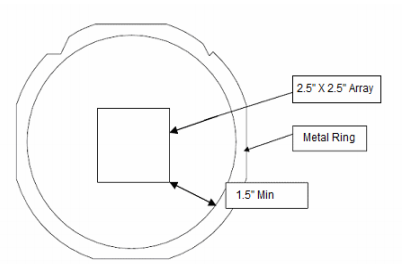
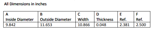
A 6 inch DTF-2-6-1 Disco or equivalent equivalent metal ring is used as a frame for partial partial wafer
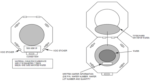
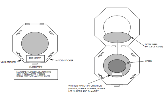
No electronic map to be provided. Sorted dice mounted on membrane with metal ring to be shipped individually in a wafer container as shown below.
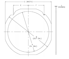
Full Wafer Packaging (For Large Quantity)
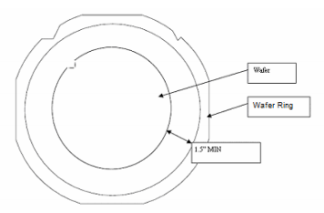
Each sawn wafer is mounted on membrane in the center of the metal ring without expansion. The distance between edge of wafer and internal metal ring has minimum 1.5" clearance. All edge dice and test-failed dice are to be black-ink marked or an Electronic Wafer map provided, see specific model data Sheet. Die sort data and electronic map to be provided in text (.txt) form upon request.
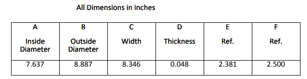
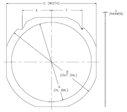
An 8 inch DTF-2-8-1 Disco or equivalent metal ring is used as a frame to mount the full wafer
The sawn wafer mounted on membrane with metal ring to be shipped individually in a wafer container as shown below.
Notes
- Known Good Dice ("KGD") means that the dice in question have been subjected to Mini-Circuits DC test performance criteria and measurement instructions and that the parametric data of such dice fall within a predefined range. While DC testing is not definitive, it does help to provide a higher degree of confidence that dice are capable of meeting typical RF electrical parameters specified by Mini-Circuits.
- Bad dice are black ink marked unless otherwise stated in model data sheet