Optimizing VCO PLL Evaluations & PLL Synthesizer Designs
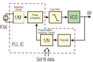
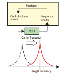
Today's mobile communications systems demand higher communication quality, higher data rates, higher frequency operation, and more channels per unit bandwidth. As much of this equipment is portable, low power consumption and small size are also required. All of these constraints combine to make the whole design including component selection and evaluation quite challenging. One portion of this design that is very critical with regard to all of the requirements mentioned above is the synthesized oscillator. Typical synthesized oscillators combine a Voltage Controlled Oscillator (VCO) with a Phase-Locked Loop IC (PLL), frequency reference (e.g. Crystal / TCXO) and a loop filter. The VCO is used to generate the RF output frequency. The PLL (which is of the "analog type"; i.e. different from a pure digital PLL) is used to stabilize and control the frequency. The loop filter design must integrate all of the components to establish, among other things, a tradeoff between noise and transient response (Figure 1). Within this paper we will describe the evaluation of the PLL and VCO and relate those evaluations to information that will allow the circuit designer to optimize the whole oscillator design including the loop filter.
VCO characteristic parameters and problems with the conventional evaluation method
Shown below are many of the common VCO evaluation parameters. To perform these evaluations, many instruments and set-ups are required even including special DC sources for both the power supply and tuning voltage.
- RF frequency [Hz]
- RF power [dBm]
- Phase noise [dBc/Hz]
- Residual FM [Hz rms]
- DC consumption current [mA]
- Tuning sensitivity [Hz/V]
- Harmonic/spurious [dBc]
- Frequency pushing [Hz/V] and frequency pulling [Hz p-p]
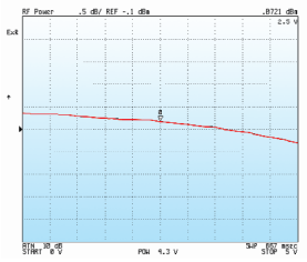
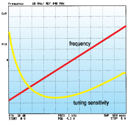
To achieve optimal circuit performance, many VCO characteristics should be evaluated under varying conditions. For example, a very fundamental parameter is the VCO output frequency versus tuning voltage (F-V). One extension of this parameter is tuning sensitivity (Hz/V), which is the differential of the F-V curve. Ideally this is a constant, but it is not. The slope change, as a function of frequency, is very important to know since this is a critical design parameter for the loop filter. But both of these parameters should also be evaluated under different power supply (Vcc) conditions since the output frequency may shift with Vcc changes. This DC power sensitivity is called frequency pushing. The RF power output will also be a function of both Vcc and output frequency. This should be evaluated since too low of an output power will result in excessive noise and too high of a level will create distortion and consume excess DC power. In addition, the DC power sensitivity has the opportunity to translate Vcc noise into modulation/noise of the oscillator output.
Many other parameters must also be evaluated; not the least of which is phase noise. Phase noise is a crucial parameter. It must be known for proper loop design and it will impact many critical operating characteristics of the synthesized oscillator including adjacent channel power.
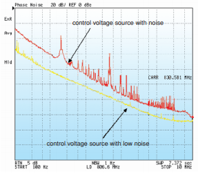
DC control voltage source noise
Noise on the DC tuning/control voltage source affects the VCO phase noise measurements since it is the VCO's job to take any control voltage variation and translate that into a frequency variation (Figure 2). For this reason the source must be very low noise, which is typically accomplished through the use of a low-pass filter. Choosing a very low cut-off frequency for this filter will yield very good noise rejection, but it will also reduce the source agility (i.e. slower frequency sweep rate) and reduce measurement accuracy. So while the filter solves some problems and may be necessary, it also creates some problems.
VCO frequency stability and phase noise characteristic evaluation
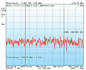
Phase noise is a random noise expressed as the ratio of the "power spectrum density at a specified offset frequency" to the "carrier signal level". This is a very sensitive measurement, so averaging is typically required to ensure measurement repeatability. Phase noise measurements can be made by both spectrum analyzers and by dedicated phase noise measurement systems.
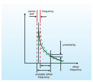
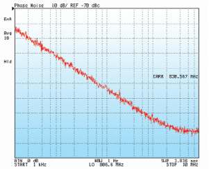
One issue with traditional phase noise measurements of the VCO is that the output frequency of these devices when they are not locked by a PLL drifts substantially over the measurement time. The VCOs are very sensitive devices and will encounter drift due to small thermal changes and even vibration. This carrier drift creates significant error that can only partially be corrected through extensive averaging (Figure 3).
Another issue is the noise measurement range. As mentioned above, spectrum analyzers can be used to measure phase noise. Aside from the drift issue mentioned above, spectrum analyzers often do not have a low enough noise floor to evaluate many of the devices required in today's communication systems.
Phase noise and phase jitter
Phase jitter causes transmit and receive timing errors and irregular sampling that results in distance, quantity, and bit errors. Phase jitter will show itself as residual phase modulation. Dedicated phase noise measurement equipment has special calculation capabilities to determine phase jitter from the phase noise measurement data.
VCO Characteristics evaluation using Agilent 4352S VCO/PLL signal test system
VCO measurement capabilities of the 4352S
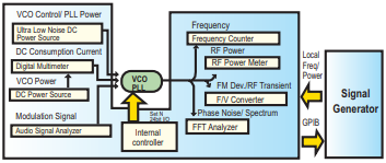
The Agilent 4352S is a self-contained solution for performing virtually all measurements required for thorough VCO evaluation (Figure 4). Specialized sources and measurement equipment have been combined to achieve this dedicated task with ease and accuracy. For example, the system contains a low noise power supply to power the DUT and an ultra low noise DC tuning / control voltage source (Figures 5 & 6). The system is integrated and includes the switching and firmware to perform all of the following tests accurately and with ease.
High speed SSB phase noise measurement function and automatic frequency control function
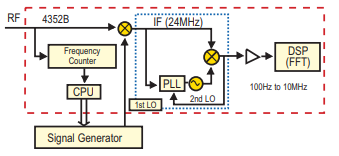
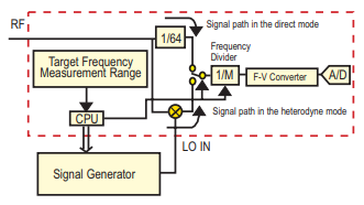
The 4352S includes a "carrier lock multi-mode PLL circuit", developed for high-speed phase noise measurements. The stepped FFT technique and the ultra low noise DC control voltage source, enable fast and easy VCO phase noise measurements. Figure 7 shows the block diagram of the carrier lock multi-mode PLL circuit. The VCO frequency is measured, and then the carrier frequency is translated into IF of 24 MHz through the mixer, with the local signal from the external signal source. The phase noise of the signal is measured in the carrier lock multi-mode PLL circuit with the orthogonal phase detection method. This phase noise measurement circuit continually locks to the drifting carrier frequency enabling quick and accurate phase noise measurement with high repeatability. Because the 4352S automatically controls all necessary settings, including the external signal source frequency, the phase noise measurement can be easily made (Figure 8).
The 4352S Automatic Frequency Control, which operates with the built-in frequency counter and DC tuning voltage source, automatically controls the DC tuning voltage. Therefore, VCO phase noise at a specific carrier frequency can easily be measured by directly entering the desired frequency (Figure 9).
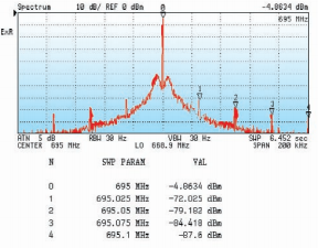
Integrated phase noise measurement function and phase jitter calculation
The 4352S can display phase noise and integrated phase noise power within the specified frequency range, on the same screen, for improved development and design efficiency. Figure 10 shows an example of an integrated phase noise measurement. (The total phase noise power [dBc] within the cursor-specified offset frequency range (1 kHz) appears at the lower left corner of the screen.)
3. PLL characteristic evaluation parameters
PLL frequency synthesizer measurement parameters
The lockup time and the spurious response of the PLL frequency synthesizer are in trade-off relationship with each other. Since a PLL frequency synthesizer typically consists of many components, it is important to consider the possible variations of each component parameter to ensure a high quality manufacturing process. The following parameters have to be evaluated for the design of an optimal loop filter, necessary in the PLL prototyping stage.
- Frequency [Hz]
- RF Power [dBm]
- Phase noise [dBc/Hz]
- Reference leak (spurious characteristic) [dBc]
- Lockup time [sec]
- Loop bandwidth
Measurement system and setup change
PLL frequency synthesizer performance evaluation generally requires a variety of measurement instruments including the following:
- Modulation domain analyzer for lockup time measurement
- Phase noise measurement system
- Spectrum analyzer for spurious characteristic evaluation
- Controller for the PLL
Performance verification of the measurement system, after every connection change, is necessary for repeatable measurements. When the loop filter characteristics or oscillation frequency is changed, measurement configurations and setup must also be changed. This tedious work may result in long product development time. Since the PLL frequency synthesizer is set to a desired frequency, by digitally controlling the PLL IC chip, a PLL control circuit or a PLL control program is necessary. It is, therefore, impossible to start the synthesizer evaluation until either the control circuit or the program is complete. Because it is difficult to synchronize measurements with a PLL frequency change, PLL lockup time measurement accuracy is difficult to achieve.
Time and frequency resolution during frequency transient measurement
PLL lockup time measurements and frequency transient analysis are conventionally performed with a modulation domain analyzer. In which case, the frequency resolution depends on the sampling interval and the measurement frequency.
4. PLL characteristic evaluation using the Agilent 4352S
All-in-one measurement system architecture
In addition to the VCO measurement functions, the 4352S can control the PLL frequency synthesizer. High-speed phase noise measurements and spectrum measurements can be made without changing connections (Figure 11). The fast phase noise measurement function greatly reduces evaluation time, subsequently improving the loop filter design efficiency.
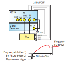
Controlling the PLL Using the IBASIC programming and 24-bit digital I/O functions
The 4352S allows the user to set a desired frequency division ratio. The IBASIC programming function and the 24-bit digital I/O port enable the lock-up time measurement to synchronize to the frequency change of the PLL synthesizer, without the need for an external PC (Figure 12).
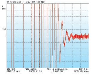
Frequency transient measurement function
Figure 13 shows the block diagram of the 4352S frequency transient measurement. The 4352S uses a frequency discriminate to convert frequency to voltage. This enables frequency transient measurements with both a time resolution of 12.5 microseconds and a frequency resolution of 50 Hz, over the entire measurement frequency range (Figure 14).
Spurious and lockup time measurement for designing loop filter
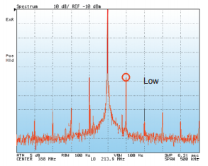
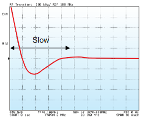
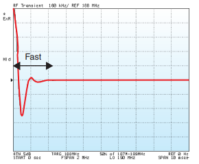
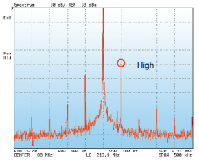
In general, the loop filter design is one of the most critical parts of the whole synthesized oscillator development. The loop filter, which is a low-pass filter inserted between the phase comparator and the VCO control voltage input terminal, eliminates the high frequency component of the phase correction pulse generated by the phase comparator so that only the DC component is provided to the VCO. In general, the lower the loop filter cutoff frequency, the more the reference leak from the phase comparator is suppressed. As a result, the PLL spurious is also suppressed as shown in Figure 15. In addition, a low loop filter cutoff frequency does not suppress phase noise at close-in offset frequencies because the closed loop negative feedback region is narrowed. It makes the PLL response slower (Figure 16) and the settling time of frequency switching (PLL lockup time) longer. Conversely, increasing cutoff frequency provides faster PLL response and shorter PLL lockup time, as shown in Figure 17. While phase noise near the carrier frequency is suppressed, the reference leak is not. It turns out that the PLL output signal is frequency-modulated and contains high level spurs (Figure 18). When performing loop filter design, it is necessary to consider phase noise, spurious, PLL lockup time tradeoffs, loop filter frequency characteristic and some design margin because even VCOs with the same specifications used in the PLL design might have slightly different characteristics. Spurious level, phase noise and frequency transient evaluation, under various conditions, bring successful PLL design and efficiency, which is crucial for shorter development time.