Switches
A wide variety of PIN diode and GaAs high-speed, high-isolation switches are available from Mini-Circuits, including models with built-in TTL drivers, operating up to 5 GHz. Select from SPST, SPDT, and SP4T models in EMI-shielded plug-in, TO-8, surface-mount and connectorized packages.
PIN diode units are available in SPST/SPDT configurations as well as SPDT/SP4T models with built-in drivers with 2 μsec switching speed, tough enough to pass stringent MIL-STD-202 tests. Despite their small size, the TO-8 models (TOSW-230 and TOSW- 425) provide isolation as high as 40 dB, only 1.1 dB insertion loss, with a 1dB compression point of +27 dBm.
Switching speed as fast as 2 nsec is offered with Mini-Circuits GaAs switches, available in absorptive and reflective models, with and without TTL built-in drivers. All models are available with SMA connectorized or surface-mount packages. The connectorized packages are miniature, easily mountable, and well suited for test set-ups. Surface-mount units are offered in a low-cost plastic package and hermetic ceramic cases for military applications. These packages are rugged enough to pass MIL-STD-883 vibration, mechanical and thermal shock, fine and gross leak tests. These fast-acting switches can operate from DC up to 5 GHz with 50dB isolation and only 1 dB insertion loss. The absorptive models exhibit a typical VSWR of 1.5 in the "OFF" state.
Modern Definition of Terms
Insertion Loss
The insertion loss is the attenuation between input and output ports of the switch when embedded in a circuit, when the switch control voltage corresponds to the "ON" state of the output port. For insertion loss measurement techniques see section O of the hand-book.
Isolation
The isolation is the attenuation between input and output ports of the switch when embedded in a circuit, when the switch control voltage corresponds to the "OFF" state of the output port. See insertion loss measurement techniques in Section O of the hand-book.
VSWR
VSWR (Voltage Standing Wave Ratio) indicates the degree of impedance match present at the switch RF port. In most cases, it is much easier to describe the impedance match in terms of return loss, dB. Return loss is equal to the amount of reflected power relative to the incident power at a port. Simply by measuring both incident and reflected power, the return loss can be measured and hence the VSWR can be calculated. For return loss measurements see section O of the handbook. For convenience, a conversion chart between VSWR and Return loss is given in section O.
Transients
During switching, video transients occur which can disturb RF components following the switch. If lower transients are critical during the switching period, use a slower transition rate between control states.
Noise Figure
Noise Figure (N.F.) of a switch is considered equal to its insertion loss.
1 dB Compression Point
The RF input power level at which the switch insertion loss increases by 1 db over its low-level value.
Switching Speed
The most popular parameters are listed below:
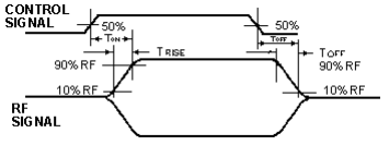
TRise = Rise Time, time for RF signal to rise from 10% to 90% of the "on" level.
TFall = Fall Time, time for RF signal to fall from 90% to 10% of the "on" level.
TOn = On Time, time from 50% of the control pulse to 90% of the "on" level.
TOff = Off Time, time from 50% of the control pulse to 10% of the "on" level. Rise time and fall time affect the upper limit of switching rate and dictate the minimum time necessary for the switch to change state. On or Off time measures the total switching time starting at control pulse transition (50% point) to RF level stabilization (90% or 10% point). Switching speed is defined as the greater of these two values.
Most Often Asked Questions About Switches
Q. What is the difference between an absorptive and a reflective switch?
A. In a reflective switch, the impedance of the port that is OFF will not be 50 ohms and will have a very high VSWR. On the other hand, an absorptive switch will have a good VSWR on each port regardless of the switch mode.
Q. Instead of working with one input and two outputs, can I use the switch in the opposite direction? I want to connect signals to the "output" ports and use the "input" as the output port
A. Yes you can. If, for example, you have two generators and want to maintain a 50-ohm load on the generator that is not switched to the common port, use an absorptive switch; otherwise, you can use a reflective switch.
Q. When should I use an absorptive switch? A reflective switch?
A. Use an absorptive switch when you need a good VSWR looking into the port that is not switched to the common port. Use a reflective switch when high OFF port VSWR does not matter and when the switch has some other desired performance feature. In most cases, an absorptive switch can be used instead of a reflective, but not vice-versa.
Q. What is the difference between PIN diode switches and GaAs switches?
A. A PIN diode switch uses the PIN diode as the nonlinear element (low impedance, current in one direction; high impedance current in the opposite direction). At frequencies above approximately 10MHz, the PIN diode moves too slowly in responding to the polarity of the RF signal, so that the diode appears as a fixed impedance (low impedance for positive DC control current, high impedance for zero current or negative DC control voltage). The GaAs switch uses a GaAs FET as the nonlinear element (the transistor being in the fully "on" or fully "off" state depending upon bias conditions).
A PIN diode switch is more tolerant of high peak power when using pulsed RF input, being limited mainly by average dissipation; power rating of a GaAs switch is determined more by internal peak voltage and current ratings. On the other hand, GaAs switches are faster, switching ON and OFF in a few nanoseconds compared with microseconds for PIN switches. Also, GaAs switches have RF response extending down to DC, whereas in PIN switches there is a practical lower limit to the frequency range in which the diodes behave as linear resistors. Finally, switching-signal (video) leakage into the RF ports is lower in GaAs switches by a factor of 10.
Q. I see that the MCL KSW and YSW series are specified down to DC. Will they actually work with DC voltage?
A. Yes, but care has to be taken to ensure that excess voltage will not burn out the switch. As a practical matter, the value of the coupling capacitors at the RF input and output of the switch will determine the lowest frequency of operation.
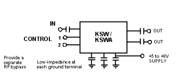
Q. I am working with a KSW/KSWA switch. Can I connect the switch to work on +V instead of - V?
A. Yes. It can be done by floating the grounds as shown in the diagram. The switch will be limited at the lower frequencies due to the blocking capacitors. Control voltages must not exceed the supply voltage.
Q. I only have -5V, not -8V. Will the KSW/ KSWA work with -5V and what will the effect be?
A. Yes, it will work but there will be as much as 6dB degradation in the 1dB compression point and the isolation between ports may degrade by a few dB.
Q. I want to use the switch as a modulator. What is the maximum modulating frequency I can use?
A. The highest modulating frequency which will switch ON and OFF fully is approximately
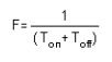
Where Ton and Toff are defined below under "switching speed." A precaution: in modulator service the maximum allowable RF input power for the KSW/KSWA/KSWHA switches is reduced as follows:
Up to 200 MHz : reduce by 10 dB
200 to 2000 MHz : reduce by 6 dB
Above 2000 MHz : reduce by 5 dB
Q. When I use the switch as a modulator, how much leakage (video break-through) of the modulating signal will appear at the output?
A. It will depend on the individual switch. GaAs switches have typically 30mV peak-to-peak leakage. PIN diode switches have typically 300mV peak-to-peak.
Q. I am using a switch to alternate between two generators. What is the isolation between the two inputs?
A. It will be close to the isolation specified between the input and output when the port is switched off.
Q. What is the peak power limit a Mini-Circuits' switch can handle?
A. Both PIN diode and GaAs chips are used as switching elements in Mini-Circuits' designs. Generally speaking, for GaAs devices the peak power will be higher at the high end of the band and will degrade as a function of frequency at about 50 to 100 MHz. The same is true with PIN diodes; however, in this case, the point of degradation occurs when the PIN diode begins to behave as a normal diode.
Q. Are Mini-Circuits' switches bi-directional?
A. Yes. From an RF point of view, input and output are interchangeable.
Q. Is the output of a switch open-circuit or closed-circuit in the "OFF" state?
A. The absorptive switch output looks like a 50-ohm impedance in the "OFF" state. A reflective switch, on the other hand, in its "OFF" state represents a high reflection which could appear as an open or a short depending on the design of the switch, the frequency involved and the length of line between the switch and the point of measurement. At low frequencies the reflective switch looks like a short.
Q. What can happen when a switch is driven into compression?
A. It will generate harmonics and insertion loss will increase.