Phase locked loop fundamentals
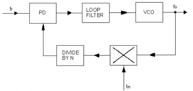
The basic form of a phase locked loop (PLL) consists of a voltage controlled oscillator (VCO), a phase detector (PD), and a filter. In its more general form (Figure 1), the PLL may also contain a mixer and a digital divider. In the steady state, the frequency of the VCO is given by the expression:
(1) fo = fm + Nfr
The frequency of the VCO may be controlled by several methods, including the following:
(i) By varying N with both fr and fm constant.
(ii) By varying fm and N with fr constant.
(iii) By varying fm and fr with N constant.
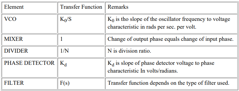
It is helpful to consider the PLL in terms of phase rather than frequency. This is done by replacing fo, fm and fr by θo, θm, θr and respectively. Table 1 shows the transfer functions of the various loop elements with this change made, and Figure 2 shows the circuit.
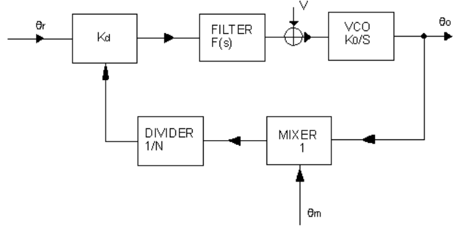
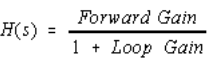
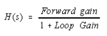
The transfer function, H(s), of a single feedback loop shown in Figure 2 is given by:
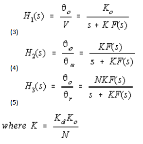
The phase of the VCO can be controlled as follows:
(i) By changing the phase, θm of the mixing frequency.
(ii) By changing the phase, θr of the reference frequency.
(iii) By changing voltage V at the modulation port.
Where V is the voltage input at the modulation port.
Taking these in turn, and making use of equation 2, we have the following equations:
and s is a complex variable used in Laplace transform and is equal to jω
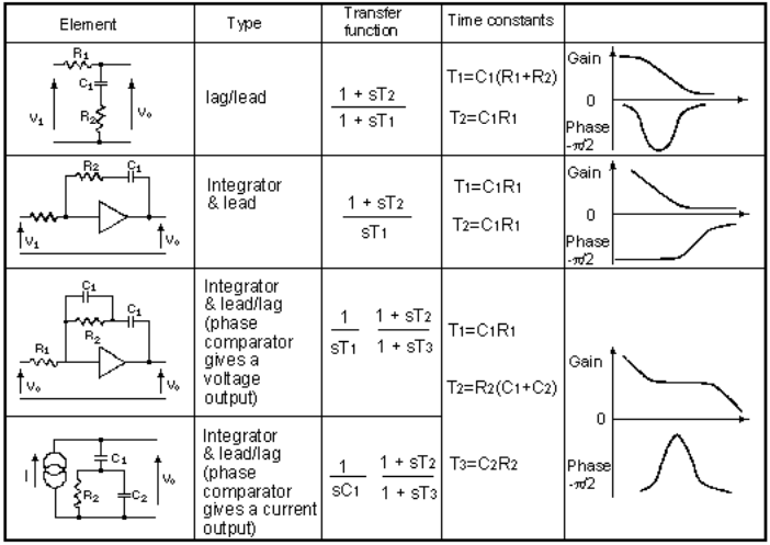
The loop filter F(s) may take one of the following forms:
(i) A lag/lead network
(ii) An integrator combined with a lead network
(iii) An integrator combined with a lead/lag network
These three forms, together with their transfer functions and Bode Diagrams, are summarized in Table 2
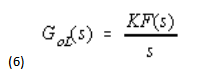
From Figure 2, it can be seen that the open loop gain is given by:
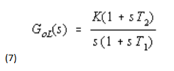
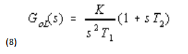
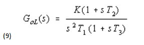
The open loop gains for the three filters shown in Table 2 are as follows:
(i) Lag/Lead filter
(ii) Integrator plus lead
(iii) Integrator plus lead/lag (voltage type phase detector)
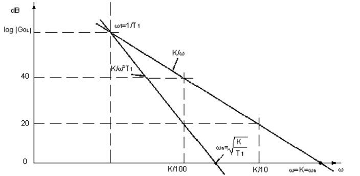
The terms K/s (equation 7) and K/S2T1 (equations 8 and 9) may be expressed, in the frequency plane, by gain lines having slopes of -20 dB/decade and -40dB/decade respectively, as shown in Figure 3.
Three very important points should be observed from the graphs:
(i) The K/ω graph has unity gain at ω = K
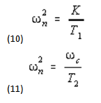
(ii) The K/ω2 T1, graph has unity gain at 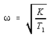 , and
, and
(iii) The two graphs meet at 
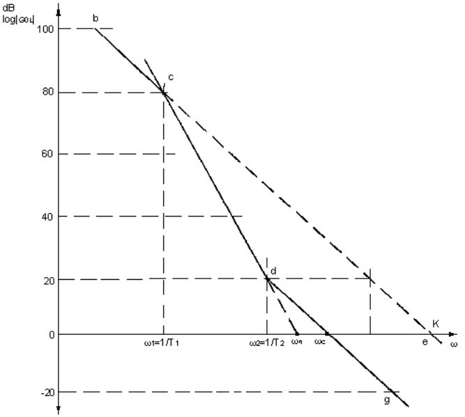
Figures 4, 5, and 6 show the effects on the open loop gain of the three filters given in Table 2.
(i) Figures 4, 5, and 6 show the effects on the open loop gain of the three filters given in Table 2.
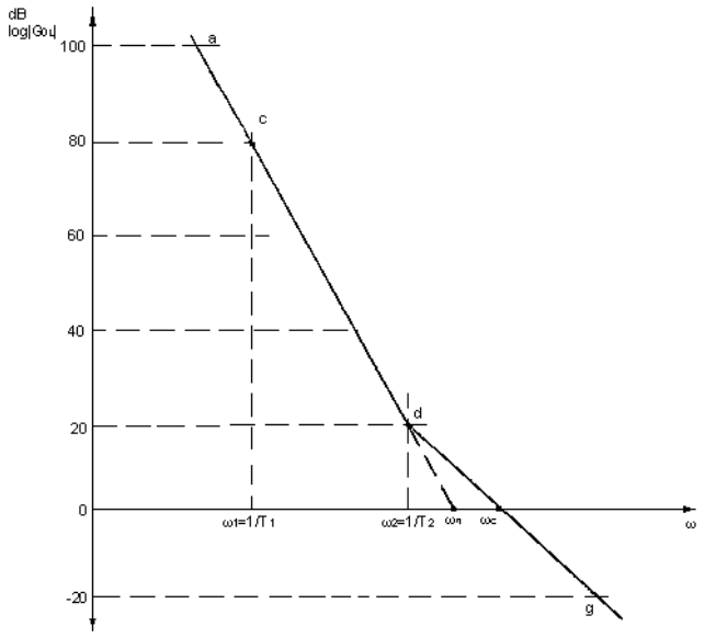
(ii) Figure 5 shows the response when the integrator plus lead network is used. In the region acd, the gain is falling at 40dB/decade.
(iii) Figure 6 shows the response when the integrator plus lead/lag network is used. In the region gh, the gain is falling at 40dB/decade. In the region dg, the gain is falling at 20dB/decade. From the foregoing, it is clear that:
(For voltage type phase detector)
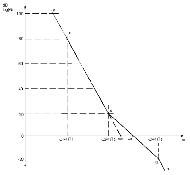
The choice of the phase detector is determined primarily by the application. For receiver applications where low noise signal levels are encountered, double balanced mixers are used as phase detectors. For synthesizer applications, a digital type phase detector is preferred. This type of phase detector produces a current output. The transfer function, Kd, has units of amps/rad. The line bcdgh in Figure 7 represents the response for this phase detector/filter combination.
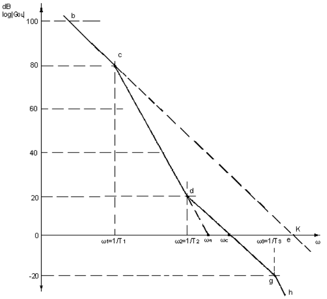
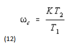
If the phase detector is not ideal but has a leakage resistance RL, then it can be shown that T1 = RLC1 and the open loop unity gain frequency (point e on Figure 7) is given by K1 = KR1. For an ideal phase detector there will be no leakage, and hence ω -> 0 and K1 -> ∞ .
From the foregoing it should be clear that both ωc and ωn can be redefined in terms of C1: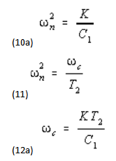
One effect of adding a filter is to reduce the open loop unity gain frequency from K(or K1) to ωc.
Frequencies below ωc will be called in-band and frequencies higher than ωc will be called out-of-band. The phase locked loop uses its in-band gain to enable the VCO to follow that of the reference frequency, and uses its out-of-band attenuation to reject unwanted phase components that may be present on the reference signal. Consequently, in most applications, the response bcdgh, given by the integrator plus lead/lag network, is preferred.
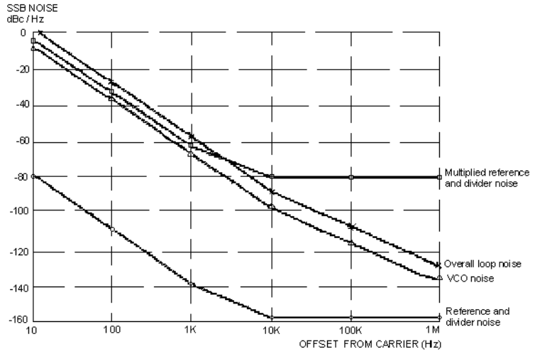
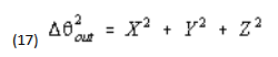
A brief analysis of the phase noise performance of the PLL is given here. The noise model is presented in Figure 8 along with the equations 14 through 17.
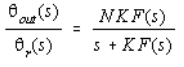
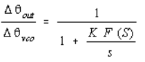
Equation 17 describes the noise output of the PLL given the noise contribution of the reference source, the phase detector, the loop filter, the VCO, and the feedback divider. The closed loop transfer function of the loop can be shown to be given by:
The loop gain G is the product of all the transfer functions, i.e.:
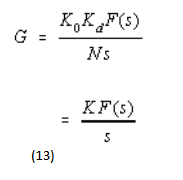
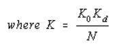
For type 2 phase locked loop, the filter consists of an integrator combined either with a lead network or with a lead/lag network.
The reference noise and the divider output noise contribution calculations follow.
The closed loop transfer function from point 1 to 4 in Figure 8 relating oscillator phase θout to reference θr to be given by:
The phase noise contributions of reference and divider noise are therefore given by:
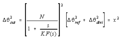
The loop division ratio must therefore be minimized so as to minimize the divider noise contributions.
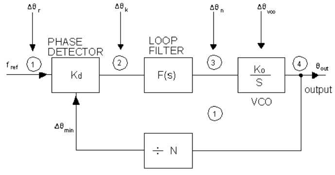
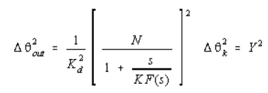
The phase detector also contributes to the output noise. In general, any noise input following the phase detector contributes to the output noise. With reference to Figure 8, the transfer function from point 2 to 4 is:
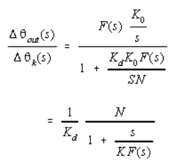
Any noise input following the phase detector is therefore inversely proportional to Kd. The noise contribution is then given by:
The phase detector gain constant must therefore be maximized so as to minimize the accompanying noise contributions. Outside the loop bandwidth, the noise will be mainly a function of the VCO. With reference to Figure 8, the transfer function from point 3 to 4 is given by:
When evaluating the output noise spectrum we must take into account the VCO noise and also its sensitivity. The following equation gives all the VCO noise contributions:
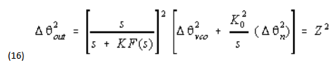
Here Ko is the VCO gain constant and Δθn any noise voltage appearing before the VCO.
The overall phase noise of the the synthesizer may be written as
The phase noise combination of the reference oscillator, dividers, and the VCO, are shown plotted in Figure 9.
In conclusion, within the loop bandwidth the reference noise will be multiplied by the loop division ratio. Outside the loop bandwidth the reference noise will be attenuated by the loop transfer function. Within the loop bandwidth, the VCO noise will be attenuated. Outside the loop bandwidth, the noise will be the same as that of the free running VCO.