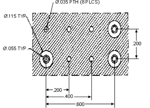
VCO Footprints
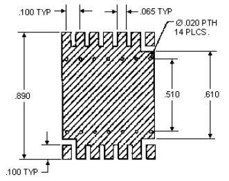
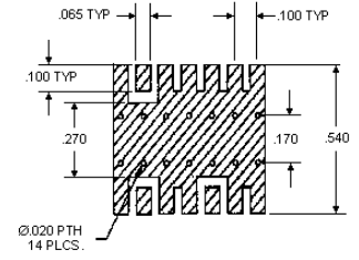
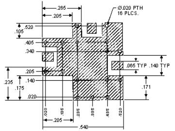
LAYOUT CONSIDERATIONS TO IMPROVE PERFORMANCE Three basic types of VCO's are manufactured by Mini-Circuits: Plug-in, Surface Mount, and Connectorized versions. To obtain the best overall performance from Mini-Circuits VCO's, good RF practices should be used. A double sided printed circuit board with plated through holes is recommended. For Mini-Circuits VCO's with "Plug-in" case style, the metallization on the top side of the PCB, on which units are mounted, should be left, as far as possible, as a continuous "ground plane" with low impedance (see Figure 1). For Mini-Circuits VCO's with "Surface Mount" case style: the metallization on the bottom side of the PCB, which is opposite to the side the VCO's are mounted, should be left as a continuous "ground plane" with low impedance (see Figures 2 through 4). For both "Plug-in" and "Surface Mount" MiniCircuitsVCO's, the printed conductors which carry RF and microwave signals (output pin of the VCO) should be designed as 50 ohm characteristic impedance microstrip lines where the width of the lines should be calculated in accordance with dielectric constant  and thickness of PCB substrate.
For PCB layouts shown in Figures 1 to 4, recommended PCB material is TaconicTM brand OAK602-0.022" with 1 ounce copper on each side. Similar material from other vendors can be used. For suggested material and thickness, the line width of the microstrip conductor should be 0.062". If the ground plane needs to be broken, it is important to support each microstrip line with a corresponding ground plane on the opposite side of the board. This ground plane should be at least three times wider than the width of the microstrip line itself. Pin Vcc should be decoupled as close as possible to the ground plane. Mini-Circuits can supply CAD drawings of recommended layouts for each model. Consult Mini-Circuits for details.