Reducing power supply noise in VCOs
Practical Techniques
It is always a good design philosophy to provide RF bypassing of power and dc control lines to the VCO. This is indeed the case when the VCO is located some distance away from the power supply.
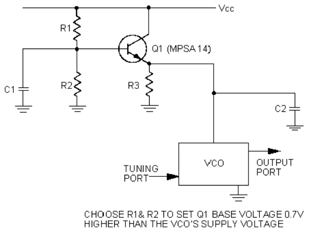
RF chokes and good bypassing capacitors of approximately 1000 pf to 0.1 μF is recommended at the DC supply lines. This will minimize the possibility of feedback between stages in a complex subsystem. Improved bypassing may be provided by incorporating an active filter circuit shown in figures 1 and 2.
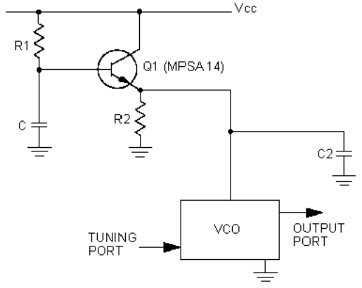
This type of RF bypassing is recommended for applications requiring a high level of noise suppression for externally generated noise signals. In most cases, the performance of the circuit in Figure 1, which is current biased, will be adequate and will have the advantage of better low frequency bypassing performance for a given value of base capacitor, fewer components, and lower power consumption.
It is only necessary to use the circuit in Figure 2 when the higher isolation offered by a larger Vcc is required. The circuit in Figure 2 is voltage biased. In this case, the circuit in Figure 2 offers a more stable operating point.
Noisy power supplies may cause additional noise. Power supply induced noise may be seen at offsets from 20 Hz to 1 MHZ from the carrier. If the VCO is powered from a regulated power supply, the regulator noise will increase depending upon the external load current drawn from the regulator. The phase noise performance of the VCO may degrade depending upon the type of regulator used, and also upon the load current drawn from the regulator. To improve the phase noise performance of the VCO under external load conditions, one or more of the following steps may be taken:
- Place a low ESR electrolytic capacitor of about 10 μF on the Vcc line (See Figure 3).
- In addition to the 10 μF capacitor mentioned in number 1 above, the decoupling of the Vcc line can be enhanced further by including a choke about 10 μH in series with the Vcc (See Figure 4).
- Provide an active bypassing as shown in Figure 1 and 2.