Digital Step Attenuators offer Precision and Linearity

Introduction
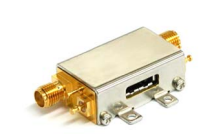
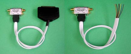
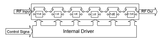
Mini-Circuits new series of digital step attenuators (DAT family) manufactured using Super RF CMOS technology, has an unprecedented combination of accuracy, linearity, programmability, ESD tolerance, and wide bandwidth in a small 4x4x0.9 mm surface mount package. This attenuator family includes models requiring only a single positive or positive-negative supply voltage. The supply voltage choice depends on switching speed and ultra low noise requirements. All Super RF CMOS Attenuators are configured as a chain of fixed attenuators with bypass switches and an internal driver for control of the switches (Fig. 1). While the Super RF CMOS Attenuator is basically a surface mount component, Mini-Circuits is also introducing a series of connectorized Super RF CMOS Attenuator models (ZX case style) for ease of connection and use in the lab, for prototyping, and in systems.
Attenuators perform the important function of amplitude control in a high-frequency system. Microwave RF attenuators are available in many different package styles and formats, including fixed-value attenuators (which are also referred to as pads), continuously variable attenuators and digitally programmable attenuators. Continuously variable attenuators, for example, are useful for emulating the propagation and multipath losses of signals between transmitters and receivers in a wireless link. Programmable attenuators are widely used in test equipment, such as signal generators, to control the output levels of test signals. Fixed attenuators are useful for improving the impedance match between components in a system, such as a filter and an amplifier, when the attenuation loss can be tolerated.
Digital attenuators have a distinguishing feature in that a known amount of attenuation can be selected at high speed according to the state of a logic signal. Digital attenuators are available commercially with and without driver circuitry. The type of logic used with the attenuator depends on the driver, with transistor-transistor logic (TTL) and most CMOS logic levels being available. When there are many bits, the external driver becomes very complex. In such cases, a significant amount of time needs to be spent by the circuit designer in implementing the driver. A multi-bit driver also increases component count, reduces reliability and occupies board space. In attenuators built using GaAs MESFET or PIN diodes, some companies incorporate the driver as a separate die inside the package at the expense of package size and increased cost. In Super RF CMOS attenuators the driver is integrated on the same die, reducing the package size, cost and complexity.
Unlike continuously variable attenuators, digital attenuators switch-in discrete, finite attenuation states, usually in binary steps. Using semiconductor devices such as GaAs MESFETs, PIN diodes or MOSFETs to achieve different attenuation states, switching can be performed at speeds comparable to solid-state switches.
Digital attenuators are specified in terms of the number of bits of attenuation, such as a 5-bit attenuator or a 6- bit attenuator. The bits do not command equal amounts of attenuation but select increasing amounts of attenuation. The least-significant bit (LSB) selects the smallest amount of attenuation offered by the component, while the most-significant bit (MSB) selects the largest amount of attenuation, with attenuation values in-between selected by the remaining bits. When all bits are selected, a digital attenuator provides its maximum rated attenuation; when only the LSB is selected, it provides its minimum attenuation step. Temperature variation of attenuation and accuracy dictate the LSB value that can be achieved, given a requirement of monotonic variation. The lower the temperature variation and the higher the accuracy, the smaller the minimum attenuation step can be, like 0.5 dB in Super RF CMOS Attenuators. In critical applications such as cellular code-division-multiple-access (CDMA) base-station transceivers, which rely on precise amplitude control, a minimum attenuation step of 0.5 dB may be required.
MSB attenuation value is dictated by the variation with temperature and frequency, and the isolation of the internal switches. It is also decided by the semiconductor process variation. Super RF CMOS Attenuators provide an MSB up to 16 dB, which is comparable or higher than the best available attenuators in the industry.
Most communication systems use 50 ohm impedance except for cable TV, where 75 ohms impedance is used. Very few manufactures cater to both impedance requirements. Super RF CMOS Attenuators are available in both impedances, 50 ohm and 75 ohm.
A digital attenuator's frequency range should be matched to the application of interest. For example, a component targeted for IEEE 802.11b/g wireless local area network (WLAN) systems should provide coverage of at least 2400 to 2500 MHz. For cellular base stations 800-1000 MHz range is required. When the frequency range of a component is broad, it can be used in many systems. This reduces the number of different components to be stocked by the user, and reduces the design time for new system, by eliminating or reducing the qualification requirement of a new component. It also results in lower cost due to large quantity purchase, which is a result of using the component in several applications. Super RF CMOS Attenuators cover a very wide frequency range. For 50 ohm systems, some Super RF CMOS Attenuator models are specified from DC to 4.0 GHz and others have useable performance over that range. These attenuators satisfy a variety of applications in wideband systems such as instrumentation, and narrow band applications including Cellular, WIMAX, PCN, UMTS, Wireless LAN, UNII, HyperLAN, and Defense communications.
For 75 ohm systems, Super RF CMOS Attenuators cover a frequency range of DC to 2.0 GHz. Applications above 1 GHz in 75 ohm systems are very few. Hence these attenuators satisfy the present and future needs of the CATV industry.
Users of digital attenuators have tended to consider them ideal in their control of signal amplitude. But these are not ideal components and, in addition to the tolerance on their nominal attenuation values, they exhibit insertion loss. One way to think of this is to consider the loss of the component when its attenuation value is set to 0 dB. Most of the insertion loss (attenuation in the 0-dB state) is due to the loss of the internal switches. In a 6 bit attenuator, the loss is due to as many as 12 SPDT switches in cascade. Design techniques and semiconductor technology dictate what can be achieved to minimize this effect. Low loss switches employed in Super RF CMOS Attenuators provide the best insertion loss in the industry.
Switching speed is another key digital attenuator parameter, and is a function of the type of active devices used, typically PIN diodes or GaAs MESFETs or CMOS. Data sheets for digital attenuators are not standardized in their representation of this performance parameter, and it is important when comparing digital attenuators to match-up switching-speed specifications fairly. One of the more common conventions is to measure a digital attenuator's switching speed in the manner of an RF switch: from 50 percent of the control signal to 90 percent of a new amplitude level. This approach considers the delays contributed by the logic driver circuitry that is usually operating with TTL or CMOS control signals. In cases where the ultimate driver speed is needed at some expense in current consumption, ECL drivers may also be considered. Super RF CMOS Attenuators are specified for 50% control to 0.5dB from the final attenuation value, which is more meaningful for the user.
A digital attenuator is specified in terms of the DC power it consumes and the RF power it handles. Depending upon the type of driver and attenuation circuitry, digital attenuators are usually designed for low-voltage (+5 VDC or less) and current consumption of 20 mA or less which is generally considered low! Many battery powered applications require lowest possible current. CMOS circuitry used in Super RF CMOS Attenuators requires negligible current (100μA) which helps to conserve battery power.
Digital attenuators are also rated for acceptable RF input power, usually in terms of the 1-dB compression point and occasionally in terms of the maximum acceptable input power level that can be tolerated without damage to the attenuator. Of course, exceeding a digital attenuator's 1-dB compression point generally results in the generation of elevated output harmonic and spurious signal levels due to the nonlinear behavior of diodes or FETs used in digital attenuators. Extreme linearity of FETs used in Super RF CMOS Attenuator results its being specified for 0.2 dB compression instead of 1 dB. Because of the linearity requirements of modern applications, digital attenuators are now often characterized in terms of their input third-order intercept point (Input IP3), with higher values denoting better linearity performance. Linearity of FETs used in Super RF CMOS Attenuator provides the best of performance over the entire band starting from 1 MHz. Digital attenuators built with MESFETs lose performance below a few hundred MHz. This is explained in paragraph 2.4
An important parameter in characterizing digital attenuators is the voltage standing wave ratio (VSWR), which is often shown as return loss. It is essentially a measure of how well the component will transfer energy with minimal reflections and power loss from and to other components in a system. When considering a wideband component for narrowband use or for multiple-frequency-band operation, it should be noted that VSWR varies as a function of frequency. Optimum performance can usually be found at midband frequencies. Some of the wideband digital attenuators industry have a return loss as poor as 11 dB, versus 20 dB typical for Super RF CMOS Attenuator which now sets the standard.
Digital attenuators are fabricated with a variety of different technologies, including monolithic chips, assemblies on low-temperature cofired ceramic (LTCC) substrates, and hybrid circuits. In most cases, specifiers will require a certain package style and footprint size for their application, and digital attenuators are available in a variety of package styles, ranging from miniature surface-mount technology (SMT) to machined-aluminum housings with coaxial connectors. Package size and style should be considered as part of a digital attenuator selection process that includes a list of environmental requirements, such as required temperature range, whether hermetic packaging is needed, and other screening requirements. Mini-Circuits digital attenuators are available in surface mount and connectorized packages to meet the needs of the customers.
Performance
Attenuation and Step Size
This DAT series of step attenuators are available in 5 and 6 bit versions with a minimum step size of 0.5 or 1 dB. Models offered, a total of 24, are shown in Table I.
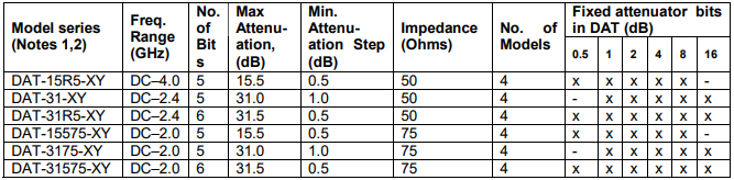
Note: 1) X = S for Serial Control and P for Parallel Control 2) Y = P for positive supply voltage (+3V) and N for dual voltage supply (± 3V)
Accuracy
A most important parameter in step attenuators is accuracy, for which Super RF CMOS Attenuators define the state-of-art. They are monotonic over the attenuation range, making them easier to program. Figure 2 graphs attenuation vs. frequency and temperature for the 0.5 dB step, showing accuracy of 0.05 dB typical from DC to 2.4 GHz.
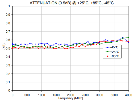
Note the accuracy change with temperature: it is within &plusmu;0.02 dB. As the step size increases the accuracy changes, but not proportionately. Figure 3 shows the accuracy for a 16 dB step.
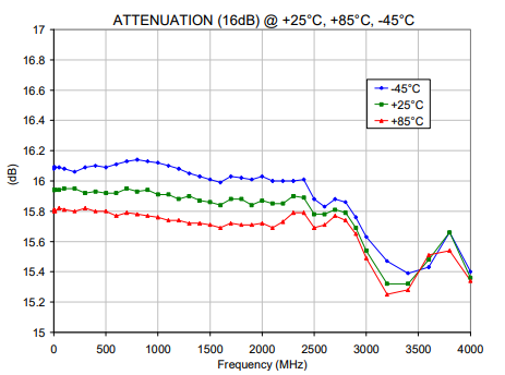
The accuracy is typically 0.1 dB from DC-1GHz and 0.15 dB from 1 to 2.5 GHz. Attenuation variation with temperature is +/- 0.2dB, which is outstanding for a big step size. Figures 2 and 3 show that the attenuators have useable performance to 4 GHz.
Impedance Match
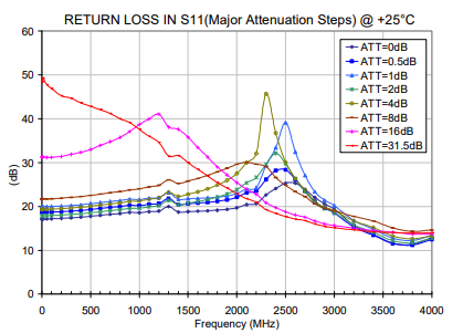
Good return loss is a requirement for accuracy. Otherwise, the impedance interactions of the attenuator and the devices interfacing with it will create an attenuation ripple. With this in mind, these attenuators have been designed for excellent return loss.
Figure 4 shows typical input return loss vs. frequency. Note the return loss is typically 18 dB or better up to 2.4 GHz for all attenuation steps.
Dynamic range
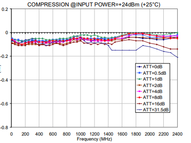
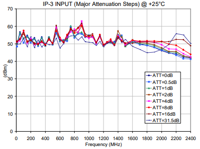
System performance is decided by the dynamic range of the individual components. High end input power level of the dynamic range of DAT attenuators is specified by compression and third-order intercept point.
One of the greatest advantages of Super RF CMOS family attenuators is its IP3 and compression, which remains substantially constant from 1 MHz to the highest specified frequency. Compare this to MESFET or PHEMT based digital attenuators, in which IP3 and compression is not constant and starts falling off below about 500 MHz as much as 20 dB!
Figure 5 shows that at +24 dBm input power the compression is typically 0.1 dB from 1 MHz to 2.4 GHz. Over a temperature range of -45° to +85°C the variation is negligible.
These attenuators offer an amazing input IP3 of 52 dBm typical from 1MHz to 2.4 GHz, as shown in Figure 6. This is better than that, which can be obtained from PIN diode based attenuators. Again, compare this to GaAs based attenuators whose IP3 starts falling below 500 MHz.
Supply Voltage
Mini-Circuits DAT family of Digital Attenuators can operate with a positive or a positive and negative supply voltage. The DAT models working with dual positive-negative supply voltage operate with switching speed of 1 MHz compared to 25 KHz for single positive supply voltage models. Customers' should select the supply voltage based on the switching frequency and noise requirements.
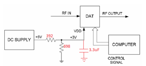
For customer applications where the system voltage is higher than the +3V specified for DAT Series Attenuators, either a LDO (Low Drop-Out) Voltage Regulator or simple Resistive Voltage Divider may be used to supply the desired voltage to the unit.
In using a resistive voltage divider to reduce the voltage from +5V to +3V, the circuit should be configured as shown below in Figure 7.
NOTE: During turn-on and transition between attenuation states, the DAT may draw up to 2mA of surge current; therefore, the equivalent voltage source should be able to source that current which requires consideration in the selection of the resistor values and the use of a shunt 3.3μF capacitor near the DAT to source current during start-up and transition
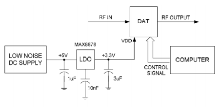
For low noise applications, and for the applications where the supply voltage varies, the customer may prefer to use a low noise LDO voltage regulator such as MAX8878 (preset to 3V), as shown in Figure 8.
Switching Control
DAT family of models have a unique CMOS circuit that allows them to be immune to latch up.
Parallel Control Models
Figure 9 is a functional schematic of 6 bit attenuator with 0.5 dB step and parallel control.
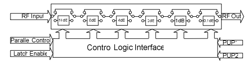
Parallel control sub family of Super RF CMOS Attenuators, can be operated in two modes: Direct parallel Programming and Latched Parallel Programming.
Direct parallel programming is useful for manual control of attenuation using hardwire, switches or jumpers. Here, latch enable is held at high state, and attenuation values change as the control signals state changes.
In latched parallel programming, latch enable is held in low state while attenuation controls are being changed. When change is complete, the latch enable state is pulsed from low to high to enable the change of attenuation and back to low to latch the change. Super RF CMOS Attenuators have a provision for setting start attenuation during power up. When the attenuator powers up with Latch Enable is set to zero state, the control bits are set to one of four possible values based on the state of the two power-up bits (PUP1 & PUP2). This defines the start up attenuation.
Serial Control Models
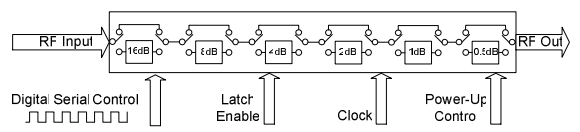
Figure 10 shows a 6 bit model with 0.5 dB step and serial control. Here attenuation is controlled by three CMOS-compatible signals: Data, Clock, and Latch Enable (LE). The Data and Clock inputs allow data to be serially entered into a built in shift register. The LE input controls the latch.
The shift register should be loaded while LE is held LOW to prevent the attenuator value from changing as data is entered. The LE input should then be toggled HIGH and brought to LOW, latching the new data. In serial mode of control, power up attenuation state is decided by the state of the six Power-Up control pins.
Further programming details are contained in the specifications for the individual models, which can be found on the Mini-Circuits website, www.minicircuits.com
Operating DAT and ZX76 Series Digital Step Attenuators when a parallel LPT port is not available
The control from the computer for the serial and parallel control interface DAT models, is done through the computer's parallel LPT port.
Some personal computers do not have parallel LPT port, which is needed to control a digital attenuator using cables and software provided by Mini-Circuits.
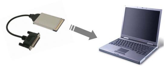
In such situations we recommend using a PCMCI (for laptop or notebook) or a PCI (for desktop PC) parallel interface card.
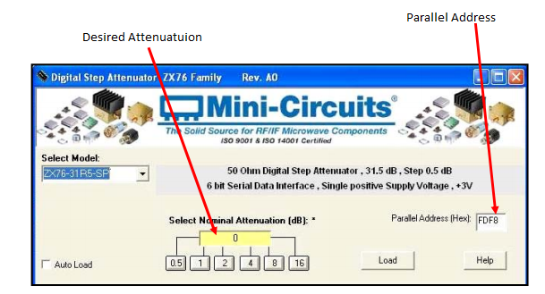
To set the correct address of the parallel card in the Mini-Circuits control software, please follow the five steps in the instructions below:
- Click Start, click Setting, click Control Panel, and then click System
- On the Hardware tab, click Device Manager. Double-click the type of parallel card that you have installed
- Click the Resources tab, and write down the first number of I/O range
- Run digital attenuator control program and enter address value in "Parallel Address" field
- Set the desired attenuation
No DC Coupling Capacitors
The internal biasing design of the Super RF CMOS Attenuators makes DC blocking capacitors at the RF ports unnecessary, caution is taken that the user's interfaces do not apply DC externally. This gives the benefit of frequency response extending down to low frequency. In contrast, any MESFET or PHEMT based step attenuators need DC blocks and the frequency response cannot go down to low frequencies.
ESD
Digital step attenuators use FETs, which are sensitive to ESD. Built-in ESD protective circuits in the DAT series of attenuators raise the immunity level to +500V per Human Body Model and +100V per Machine Model. This makes them capable of being used with only standard ESD precautions.
Switching Speed
These attenuators have a switching time of 1μs. It is an industry standard convention to define switching time as 50% control to 10 to 90% of RF. GaAs attenuators, have a long tail after 90% for rising signals and before 10% for falling signals. Hence the time necessary to reach the final value of attenuation is much higher and is comparable to Super RF CMOS Attenuators.
Positive voltage models can work with a switching control frequency of ~25KHz. Increasing the switching control frequency above ~25KHz will affect the Rise/Fall time, which will affect how fast the DAT changes attenuation values. This phenomenon will appear more drastically above 200 KHz. Dual voltage models can work with a switching control frequency up to 1MHz without degradation in Rise/Fall time. Above 1MHz there will be same degradation as explained above.
Conclusions
A series of Digital Step Attenuators (24 models) have been introduced, which define the state-of-art. A unique combination of accuracy, linearity, programmability, ESD tolerance, positive supply voltage and wide bandwidth in a small size make them unique in the industry. 50 and 75 ohm models are offered to serve the need for digital step attenuators in wide band and narrow band applications up to 4 GHz. All Mini-Circuits Super RF CMOS Attenuator models are immune to "latch up" which is a problem with conventional CMOS circuits.