Specifying VCOs for Clock Timing Circuits
Ted Heil, President
Erick A. Olsen, Product Marketing Manager
Mini-Circuits, 13 Neptune Ave., Brooklyn, NY 11235; www.minicircuits.com
VCOs are capable of low noise and high stability with the convenience of tunable frequency for applications requiring reliable clock timing.
Timing is everything for many systems, especially for modern electronic systems with high-speed data converters and high-resolution sampling. A clock source is "the keeper of time" in these systems and system timing performance is very much dependent upon the performance of its clock source. For some system designers, a clock source automatically means a crystal oscillator, typically a single-frequency source. But some system designers, especially those faced with synchronizing systems at multiple clock frequencies, have learned to appreciate the flexibility of using voltage-controlled oscillators (VCOs) as clock sources.
VCOs can serve as clock timing circuits for wireless communications networks, video broadcast systems, and test equipment, essentially any systems requiring timing synchronization, for data processing, digital signal processing, or channeling of logic signals. VCOs support data-conversion circuits in analog-to-digital converters (ADCs), digital-to-analog converters (DACs), and logic circuits in need of reliable clock timing signals. These tunable, high-frequency oscillators are available from many different suppliers in many different formats, from chips to packaged devices, making the task of specifying a VCO for a clock timing application or even a traditional analog heterodyne receiver no simple task. Selecting a VCO for clock timing applications requires an understanding of VCO performance specifications and how they can be applied in the time-domain realm of clock timing circuits.
Working with clock timing circuits usually involves tight management of timing accuracy in the clock timing source. Errors in clock timing can result in poor digital system performance, causing lost or missing data. High-speed clock signals are usually characterized by fast rise and fall times, with an amplitude-versus-time plot showing a peak amplitude with very sharp edges (Fig. 1). Sharper slopes leading to and trailing from the peak amplitude represent less noise and less timing errors. Clock signals that are narrower or wider than optimum limits are errors in clock timing caused by phase noise and can degrade system performance.
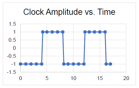
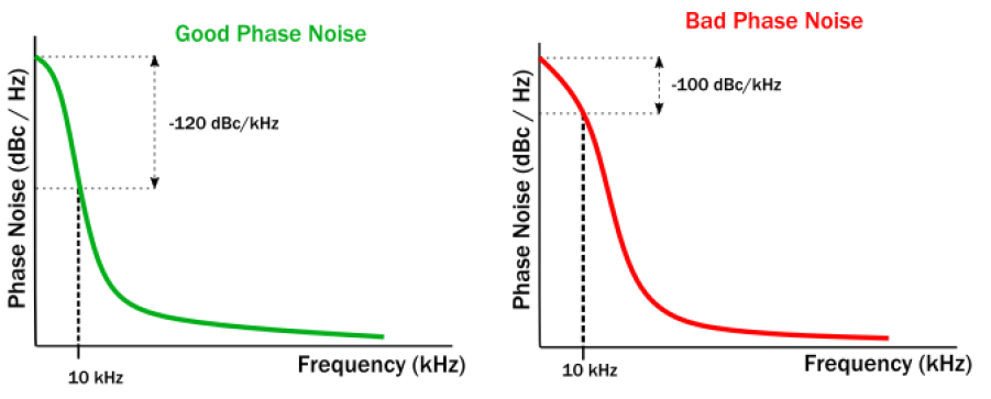
An ideal clock signal plot would show a signal trace with almost vertical, 90° rising and falling edges to the peak amplitude of the output signal. Unfortunately, real-world clock oscillators suffer some amount of noise due to signal power spread from the carrier to the sidebands as well as the generation of harmonics of the desired output frequency. Noise can also result from nonharmonic, spurious signal sources falling within the bandwidth of the oscillator. Additionally, energy spread from the carrier to the sidebands causes variations in signal frequency and phase and is measured as single-sideband (SSB) phase noise (Fig. 2). All these noise sources can cause timing errors in an oscillator that is used as a clock source.
While no ideal clock timing source may exist, good sources are available. Oscillator noise parameters of SSB phase noise, harmonic noise, and spurious noise provide a means to determine the usefulness of a given model as a clock timing source. VCOs provide output signals at a specified center frequency (fc) and modulation bandwidth around that center frequency. A VCO's tuning range is defined by a minimum and maximum frequency and by the tuning voltage that is applied to the oscillator to produce the frequencies within its tuning range.
Asynchronous clocking applications, such as video broadcast systems and Ethernet systems, typically employ many different clock oscillators serving as local timing reference sources for different components (such as ADCs, DACs, and FPGAs) within the system. For such applications requiring multiple clock signals, the frequencies of those clock signals will establish a minimum tuning range for a VCO used as a clock oscillator, perhaps with added bandwidth to allow for some amount of frequency tolerance within the system. The VCO's tuning step size should provide the frequency resolution (such as 1 kHz) required to produce the frequencies of the multiple timing signals. Commercial VCOs are available with both narrowband and wideband tuning ranges, although the tuning response must provide the frequency resolution required by a given application.
The frequency control of a VCO is also defined by its tuning speed, which is typically the time for an oscillator to settle within 90% of its final frequency after a change in tuning voltage has been applied. The tuning speed may also be described by a VCO's settling time, which is a function of modulation bandwidth (longer settling times for wider bandwidths).
Additional VCO frequency-tuning parameters to consider include:
- post-tuning drift: variations from a desired frequency within a specified time after a tuning voltage has been applied;
- frequency pushing: variations from a desired frequency due to changes in power-supply voltage, usually expressed as MHz/V; and
- frequency pulling: variations from a desired frequency as a result of impedance loads from other components within the same system, such as amplifiers and filters connected to the VCO.
For systems with multiple VCOs, pulling can cause frequency errors and timing differences between clock oscillators that can impact bit error rate (BER) and digital system performance.
Controlling Noise and Jitter
For high-speed clock timing circuits, clock timing oscillators should provide high stability, with the lowest levels of noise possible, including low SSB phase noise, harmonics, and spurious noise. All three forms of noise can degrade system-level performance when a VCO is used as a clock timing oscillator. In the frequency domain, SSB phase noise close to the carrier (such as offset 1 or 10 kHz from the carrier) is usually considered of most concern because it is often being mixed with the carrier as a local oscillator (LO) for receiver or transmitter frequency-conversion applications. In the time domain, where phase noise is referred to as "jitter," high noise levels at offsets further from the carrier are also of greater concern because they are an indication of large amounts of wideband noise. When phase noise is represented as jitter, it is the total integrated phase noise (noise at all offsets) that is considered for jitter conversions and noise far from the carrier can contribute to increased jitter. Especially for VCOs used as clock sources, noise far from the carrier can be thought of as degrading the rise and fall times or sharpness of a clock's pulse edges, resulting in timing errors.
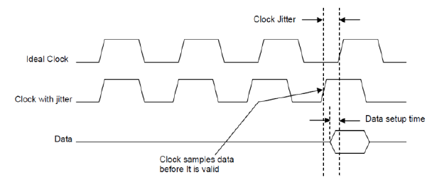
Jitter refers to timing variations in the signal edges of an oscillator's clock signals when compared to perfectly timed clock signals (Fig. 3). The signal timing variations are caused by noise within a system and can be the result of the effects of changing operating temperatures, power-supply variations, changes in the impedance load conditions, semiconductor device noise, and interference from nearby circuits. When considering a VCO for clock timing applications, whether it be phase noise or jitter, the value should be as low as possible for the most precise timing results. In general, a VCO with acceptably low phase noise will also perform with very low jitter in clock timing circuits. The additional oscillator noise components from harmonic and spurious signals can also degrade the quality of oscillator spectral purity in the frequency domain and jitter performance in the time domain and should be kept at the lowest levels possible.
Comparing the phase-noise levels of different VCOs for clock timing applications is typically not a simple task since the phase noise occupies so many different sidebands around a carrier frequency (fc) of interest. Phase noise is typically at its highest levels close to the carrier, with noise levels dropping for offsets further from the carrier. The phase noise typically has three slopes, with the highest slope, for noise also known as flicker FM noise, close to the carrier. The middle slope region of phase noise is known as 1/f noise, with steadily decreasing noise further from the carrier. The region of phase noise furthest from the carrier, at the lowest levels of noise, is known as white noise or broadband noise. Because jitter equates to the total integrated phase noise of an oscillator, higher broadband phase noise contributes to higher jitter. High jitter causes errors in digital system sampling time, reduced signal-to-noise ratio (SNR) and missing or lost digital bits.
Measurements of phase noise are performed in one of the sidebands (>fc or >fc) within a 1-Hz bandwidth at various offsets from the carrier frequency. It is important that the noise levels being compared for different oscillators are for the same carrier frequency and offsets. Because the noise power is at frequencies lower or higher than the desired carrier, high phase noise results in some "detuning" of the carrier frequency, depending upon the sideband and the offset frequency. For clock timing applications, the SSB phase-noise levels across all offsets from the carrier are important, especially at offsets greater than 10 MHz (which are often not considered for analog applications). In short, lower levels of SSB phase noise equal low jitter in VCOs.
Connecting a VCO
Analog circuit designers have long applied VCOs' outputs to heterodyne receiver ports as LO signals, converting RF input signals to intermediate-frequency (IF) signals for processing. In the mixed-signal and digital circuit realms, components such as digital signal processors (DSPs), ADCs, and DACs provide clock input ports for timing and synchronization purposes. Signals for these clock inputs have traditionally been provided by lower-frequency clock oscillators. But as the speeds and frequencies of digital components continue to climb, VCOs appear as more likely candidates for clock timing sources because they provide the higher frequencies, lower phase noise, and outstanding stability needed for clock timing circuits. The impact of VCO performance on analog systems is well understood, and VCOs can be just as valuable as timing sources for digital systems.
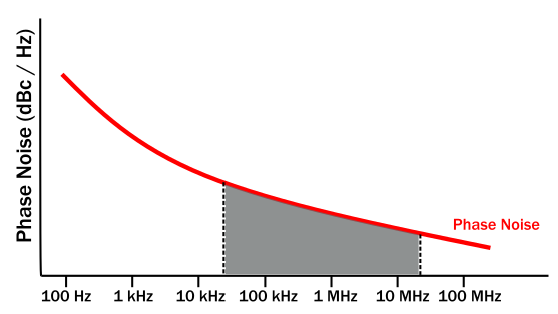
Fortunately, VCO phase-noise plots and an oscillator's spectral purity (including harmonics and spurious noise) can be translated into jitter for clock timing applications using equations available in the literature or a jitter mask which is imposed over a VCO's phase-noise plot to identify noise at offset frequencies of interest. The phase noise may not be critical at all offsets; for example, noise at offsets from 12 kHz to 20 MHz has traditionally been of main concern for optical communications applications such as synchronous optical network (SONET) communications systems. In general, a jitter mask (Fig. 4) can be a useful tool for identifying design limits, such as the maximum SSB phase noise levels corresponding to required jitter design limits in the time domain.
Sizing Up Specs
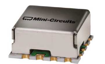
What type of VCO performance levels are needed for providing dependable clock timing in real-world applications? For a sampling of VCOs developed for clock timing applications, see the table. Model 4608CH-2+ is a fixed-frequency oscillator developed to provide a fixed timing signal at 4608 MHz for cable television (CATV) systems. It is housed in a compact surface-mount package (Fig. 5) for operating temperatures from -5 to +95°C.
At less than one-half the frequency, model ROS-1801C-1+ provides clock timing signals at 1800 MHz as a drop-in replacement for fixed-frequency integrated-circuit (IC) VCOs in many test equipment and system applications. It provides as much as +8 dBm output power and typically +6 dBm output power with typical tuning sensitivity of 1.5 MHz/V for a tuning-voltage range of 0.5 to 9.5 V.
At 2000 MHz, model ROS-2000C-6+ is a VCO well suited for clock timing applications in emerging Fifth Generation (5G) clock timing applications. The RoHS-compliant source is also housed in a compact surface-mount package, with very little drift across a wide operating temperature range of -40 to +85°C. All three VCOs feature low phase noise and outstanding frequency stability to serve as clock timing sources.
In short, electronic systems continue to move higher in frequency and speed, with growing numbers of users relying on those systems for communications, transportation, even health care. To keep users and their systems connected, timing is everything, and electronic timing depends on a high-quality clock source, often more than one. For higher system frequencies, low-noise VCOs provide the timing accuracy needed to maintain many systems well into the future.
Note: For more on VCO performance parameters, refer to "Glossary of VCO Terms" on minicircuits.com. For more on VCO testing, refer to "Mini-Circuits® VCO Test Methods."